38.3.4 Interrupt Delay register (PDBx_IDLY)
Note: This register is internally buffered, and any values written to the register are
written to its internal buffer instead; in other words, the internal device bus does not write
directly to this register. The value in this register's internal buffer is loaded into this
register only after "1" is written to the SC[LDOK] bit.
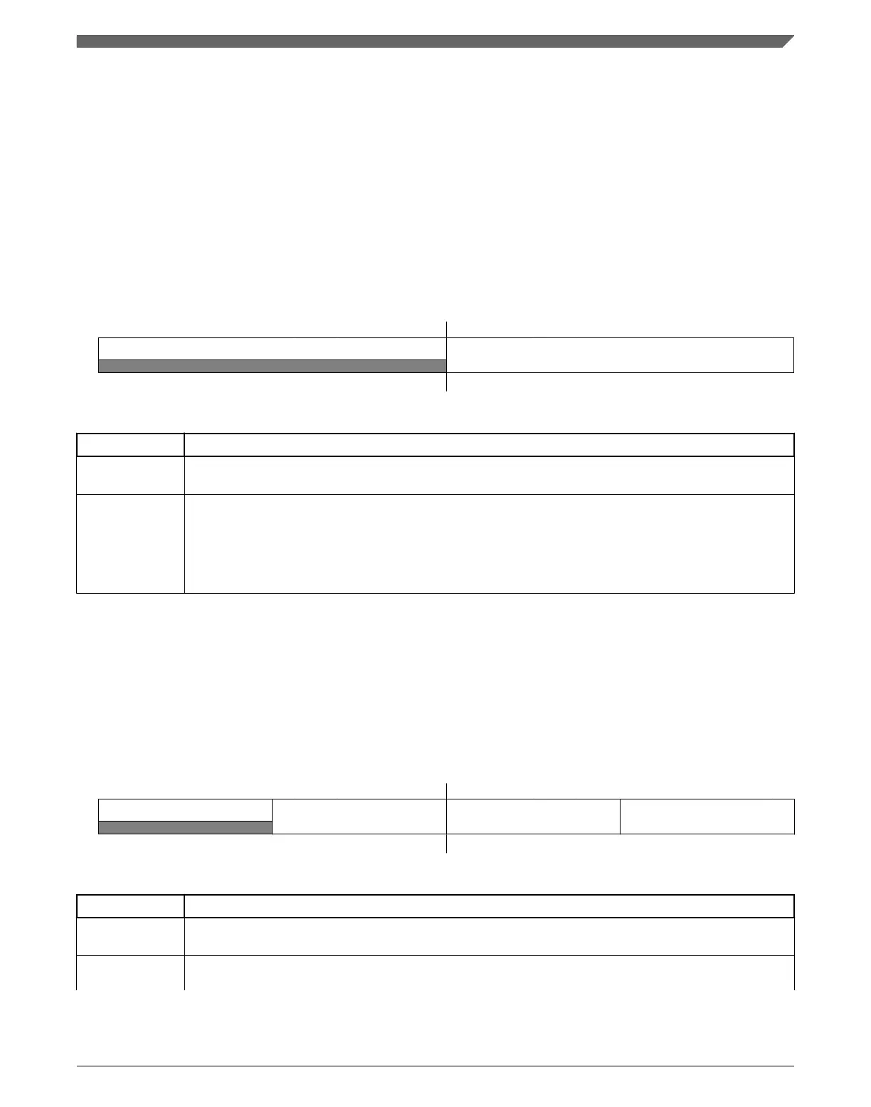
Address:
4003_6000h base + Ch offset = 4003_600Ch
Bit 31 30 29 28 27 26 25 24 23 22 21 20 19 18 17 16 15 14 13 12 11 10 9 8 7 6 5 4 3 2 1 0
R
0
IDLY
W
Reset
0 0 0 0 0 0 0 0 0 0 0 0 0 0 0 0 1 1 1 1 1 1 1 1 1 1 1 1 1 1 1 1
PDBx_IDLY field descriptions
Field Description
31–16
Reserved
This field is reserved.
This read-only field is reserved and always has the value 0.
IDLY PDB Interrupt Delay
Specifies the delay value to schedule the PDB interrupt. It can be used to schedule an independent
interrupt at some point in the PDB cycle. If enabled, a PDB interrupt is generated, when the counter is
equal to the IDLY. Reading this field returns the value of internal register that is effective for the current
cycle of the PDB.
38.3.5 Channel n Control register 1 (PDBx_CHnC1)
Each PDB channel has one control register, CHnC1. The bits in this register control the
functionality of each PDB channel operation.
Address:
4003_6000h base + 10h offset + (40d × i), where i=0d to 1d
Bit 31 30 29 28 27 26 25 24 23 22 21 20 19 18 17 16 15 14 13 12 11 10 9 8 7 6 5 4 3 2 1 0
R
0
BB TOS EN
W
Reset
0 0 0 0 0 0 0 0 0 0 0 0 0 0 0 0 0 0 0 0 0 0 0 0 0 0 0 0 0 0 0 0
PDBx_CHnC1 field descriptions
Field Description
31–24
Reserved
This field is reserved.
This read-only field is reserved and always has the value 0.
23–16
BB
PDB Channel Pre-Trigger Back-to-Back Operation Enable
Table continues on the next page...
Chapter 38 Programmable Delay Block (PDB)
K22F Sub-Family Reference Manual, Rev. 4, 08/2016
NXP Semiconductors 877

 Loading...
