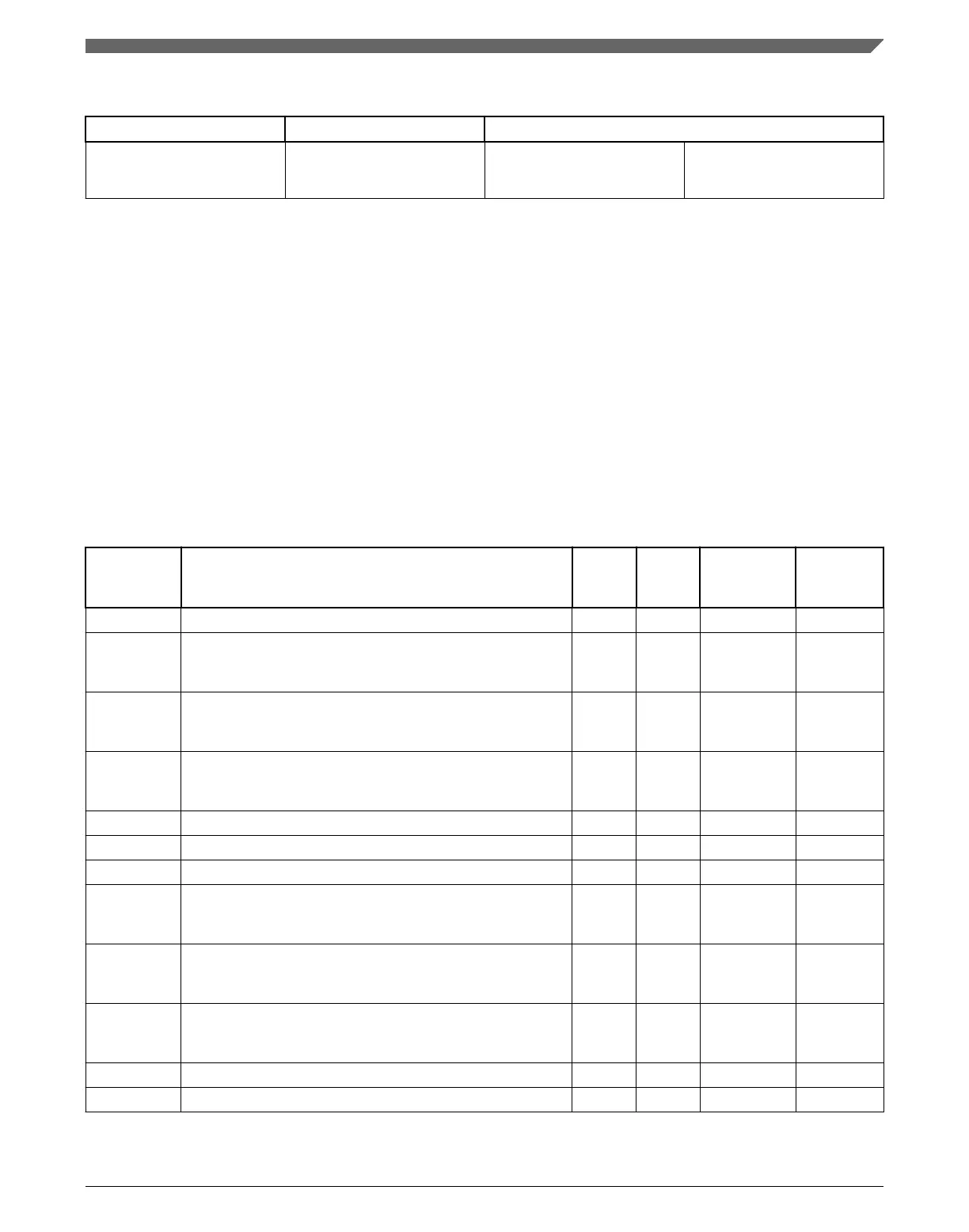
Table 50-3. GPIO interface-detailed signal descriptions
Signal I/O Description
at any time and input may be
asserted asynchronously to
the system clock.
NOTE
Not all pins within each port are implemented on each device.
See the chapter on signal multiplexing for the number of GPIO
ports available in the device.
50.2
Memory map and register definition
Any read or write access to the GPIO memory space that is outside the valid memory
map results in a bus error.
GPIO memory map
Absolute
address
(hex)
Register name
Width
(in bits)
Access Reset value
Section/
page
400F_F000 Port Data Output Register (GPIOA_PDOR) 32 R/W 0000_0000h 50.2.1/1378
400F_F004 Port Set Output Register (GPIOA_PSOR) 32
W
(always
reads 0)
0000_0000h 50.2.2/1379
400F_F008 Port Clear Output Register (GPIOA_PCOR) 32
W
(always
reads 0)
0000_0000h 50.2.3/1380
400F_F00C Port Toggle Output Register (GPIOA_PTOR) 32
W
(always
reads 0)
0000_0000h 50.2.4/1380
400F_F010 Port Data Input Register (GPIOA_PDIR) 32 R 0000_0000h 50.2.5/1381
400F_F014 Port Data Direction Register (GPIOA_PDDR) 32 R/W 0000_0000h 50.2.6/1381
400F_F040 Port Data Output Register (GPIOB_PDOR) 32 R/W 0000_0000h 50.2.1/1378
400F_F044 Port Set Output Register (GPIOB_PSOR) 32
W
(always
reads 0)
0000_0000h 50.2.2/1379
400F_F048 Port Clear Output Register (GPIOB_PCOR) 32
W
(always
reads 0)
0000_0000h 50.2.3/1380
400F_F04C Port Toggle Output Register (GPIOB_PTOR) 32
W
(always
reads 0)
0000_0000h 50.2.4/1380
400F_F050 Port Data Input Register (GPIOB_PDIR) 32 R 0000_0000h 50.2.5/1381
400F_F054 Port Data Direction Register (GPIOB_PDDR) 32 R/W 0000_0000h 50.2.6/1381
Chapter 50 General-Purpose Input/Output (GPIO)
K22F Sub-Family Reference Manual, Rev. 4, 08/2016
NXP Semiconductors 1377

 Loading...