3.7.3.3 12-bit DAC Reference
For this device VREF_OUT and VDDA are selectable as the DAC reference.
VREF_OUT is connected to the DACREF_1 input and VDDA is connected to the
DACREF_2 input. Use DACx_C0[DACRFS] control bit to select between these two
options.
Be aware that if the DAC and ADC use the VREF_OUT reference simultaneously, some
degradation of ADC accuracy is to be expected due to DAC switching.
3.7.4
VREF Configuration
This section summarizes how the module has been configured in the chip. For a
comprehensive description of the module itself, see the module’s dedicated chapter.
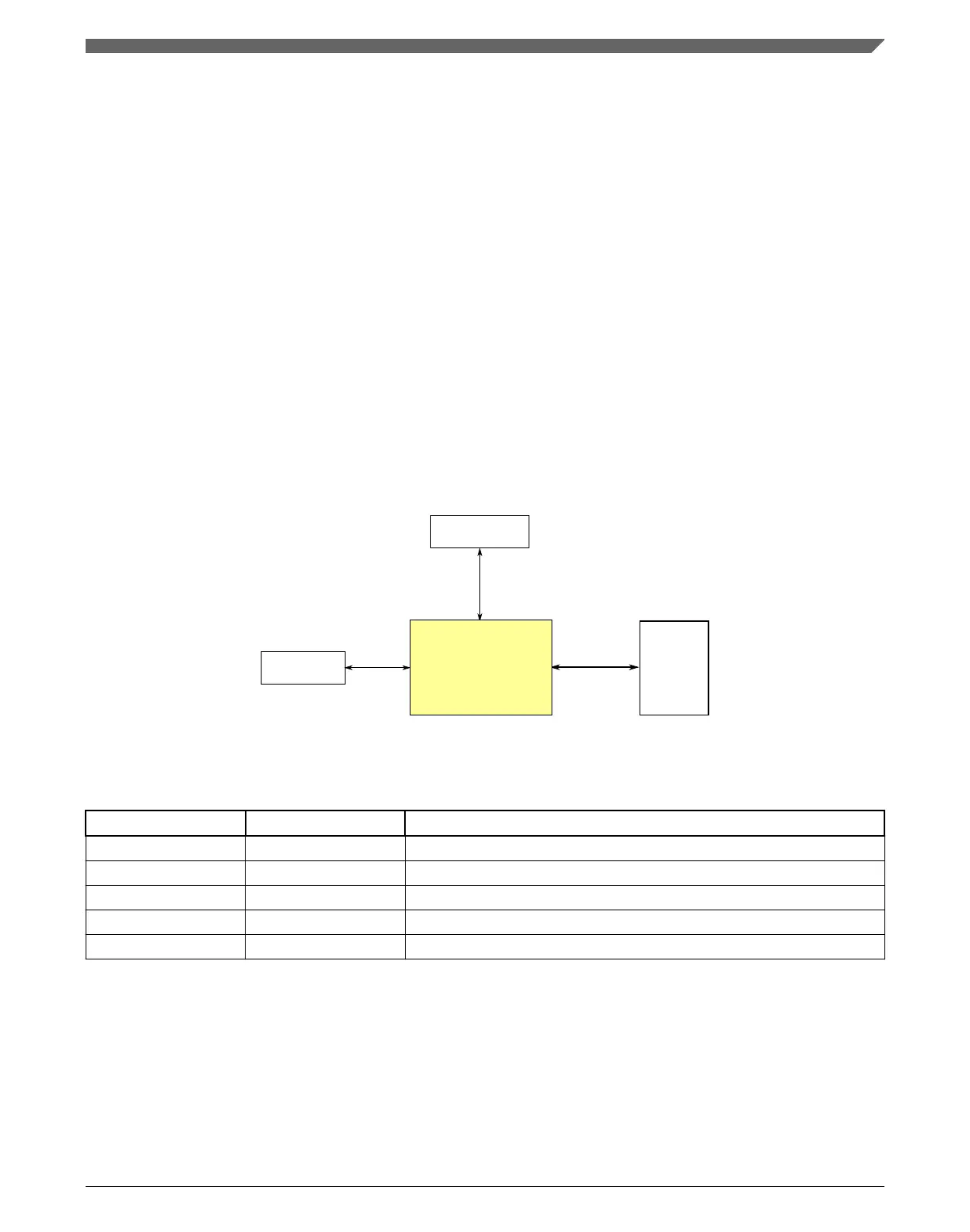
Signal
multiplexing
Module signals
Register
access
VREF
Peripheral bus
controller 0
Other
peripherals
Transfers
Figure 3-35. VREF configuration
Table 3-49. Reference links to related information
Topic Related module Reference
Full description VREF VREF
System memory map System memory map
Clocking Clock distribution
Power management Power management
Signal multiplexing Port control Signal multiplexing
3.7.4.1 VREF Overview
This device includes a voltage reference (VREF) to supply an accurate 1.2 V voltage
output.
Chapter 3 Chip Configuration
K22F Sub-Family Reference Manual, Rev. 4, 08/2016
NXP Semiconductors 107

 Loading...