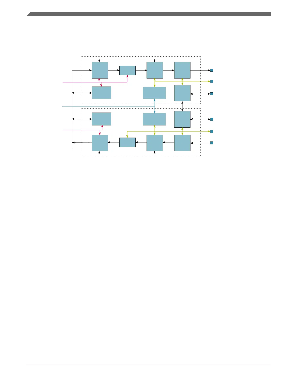
49.1.2 Block diagram
The following block diagram also shows the module clocks.
Write
FIFO
Control
FIFO
Read
FIFO
Control
Shift
Register
Control
Registers
Bit Clock
Generation
Frame
Sync
Control
Control
Registers
Bit Clock
Generation
Frame
Sync
Control
Read
FIFO
Control
FIFO
Write
FIFO
Control
Shift
Register
Bus
Clock
Audio
Clock
Bit
Clock
Bus
Clock
Transmitter
Receiver
Synchronous Mode
SAI_TX_DATA
SAI_TX_BCLK
SAI_TX_SYNC
SAI_RX_SYNC
SAI_RX_BCLK
SAI_RX_DATA
Bit
Clock
Figure 49-1. I
2
S/SAI block diagram
49.1.3
Modes of operation
The module operates in these power modes: Run mode, stop modes, low-leakage modes,
and Debug mode.
49.1.3.1
Run mode
In Run mode, the SAI transmitter and receiver operate normally.
49.1.3.2
Stop modes
In Stop mode, the SAI transmitter and/or receiver can continue operating provided the
appropriate Stop Enable bit is set (TCSR[STOPE] and/or RCSR[STOPE], respectively),
and provided the transmitter and/or receiver is/are using an externally generated bit clock
or an Audio Master Clock that remains operating in Stop mode. The SAI transmitter
and/or receiver can generate an asynchronous interrupt to wake the CPU from Stop mode.
Introduction
K22F Sub-Family Reference Manual, Rev. 4, 08/2016
1338 NXP Semiconductors

 Loading...