SIM_SCGC6 field descriptions (continued)
Field Description
0 Clock disabled
1 Clock enabled
12.2.12 System Clock Gating Control Register 7 (SIM_SCGC7)
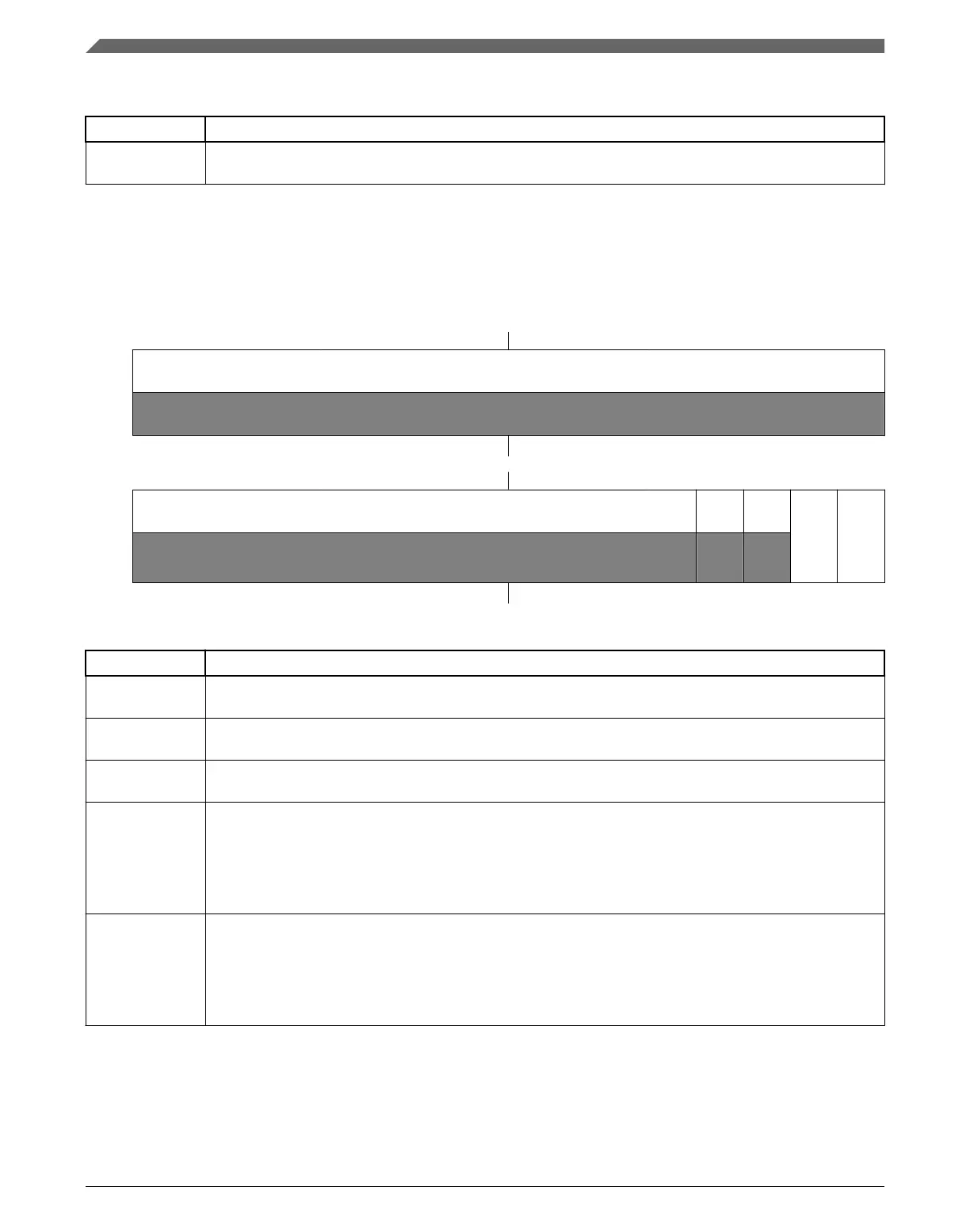
Address: 4004_7000h base + 1040h offset = 4004_8040h
Bit 31 30 29 28 27 26 25 24 23 22 21 20 19 18 17 16
R
0
W
Reset
0 0 0 0 0 0 0 0 0 0 0 0 0 0 0 0
Bit
15 14 13 12 11 10 9 8 7 6 5 4 3 2 1 0
R
0 0 0
DMA
FLEXBUS
W
Reset
0 0 0 0 0 0 0 0 0 0 0 0 0 0 1 0
SIM_SCGC7 field descriptions
Field Description
31–4
Reserved
This field is reserved.
This read-only field is reserved and always has the value 0.
3
Reserved
This field is reserved.
This read-only field is reserved and always has the value 0.
2
Reserved
This field is reserved.
This read-only field is reserved and always has the value 0.
1
DMA
DMA Clock Gate Control
This bit controls the clock gate to the DMA module.
0 Clock disabled
1 Clock enabled
0
FLEXBUS
FlexBus Clock Gate Control
This bit controls the clock gate to the FlexBus module.
0 Clock disabled
1 Clock enabled
Memory map and register definition
K22F Sub-Family Reference Manual, Rev. 4, 08/2016
284 NXP Semiconductors

 Loading...