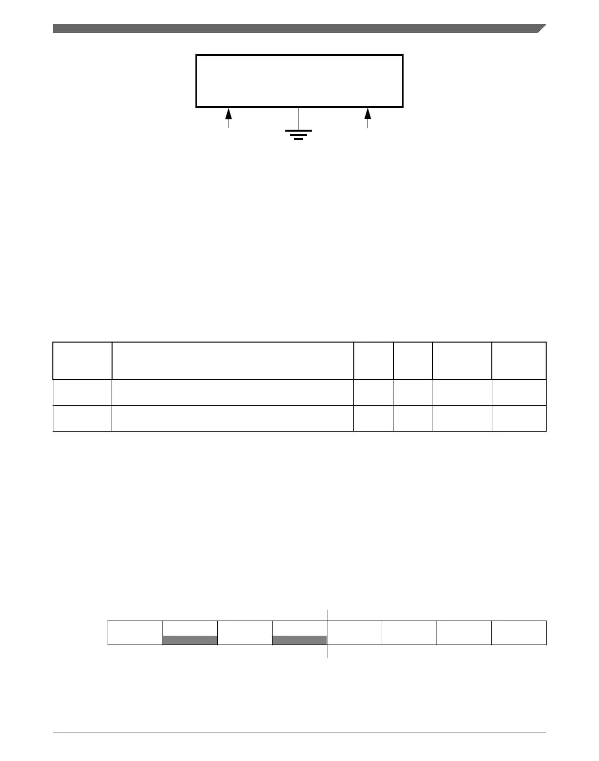
OSC
VSS
Clock Input
I/O
XTAL
EXTAL
Figure 26-5. External Clock Connections
26.7 Memory Map/Register Definitions
Some oscillator module register bits are typically incorporated into other peripherals such
as MCG or SIM.
OSC Memory Map/Register Definition
OSC memory map
Absolute
address
(hex)
Register name
Width
(in bits)
Access Reset value
Section/
page
4006_5000 OSC Control Register (OSC_CR) 8 R/W 00h
26.7.1.1/
581
4006_5002 OSC_DIV (OSC_OSC_DIV) 8 R/W 00h
26.7.1.2/
583
26.7.1.1 OSC Control Register (OSC_CR)
NOTE
After OSC is enabled and starts generating the clocks, the
configurations such as low power and frequency range, must
not be changed.
Address:
4006_5000h base + 0h offset = 4006_5000h
Bit 7 6 5 4 3 2 1 0
Read
ERCLKEN
0
EREFSTEN
0
SC2P SC4P SC8P SC16P
Write
Reset
0 0 0 0 0 0 0 0
26.7.1
Chapter 26 Oscillator (OSC)
K22F Sub-Family Reference Manual, Rev. 4, 08/2016
NXP Semiconductors 581

 Loading...