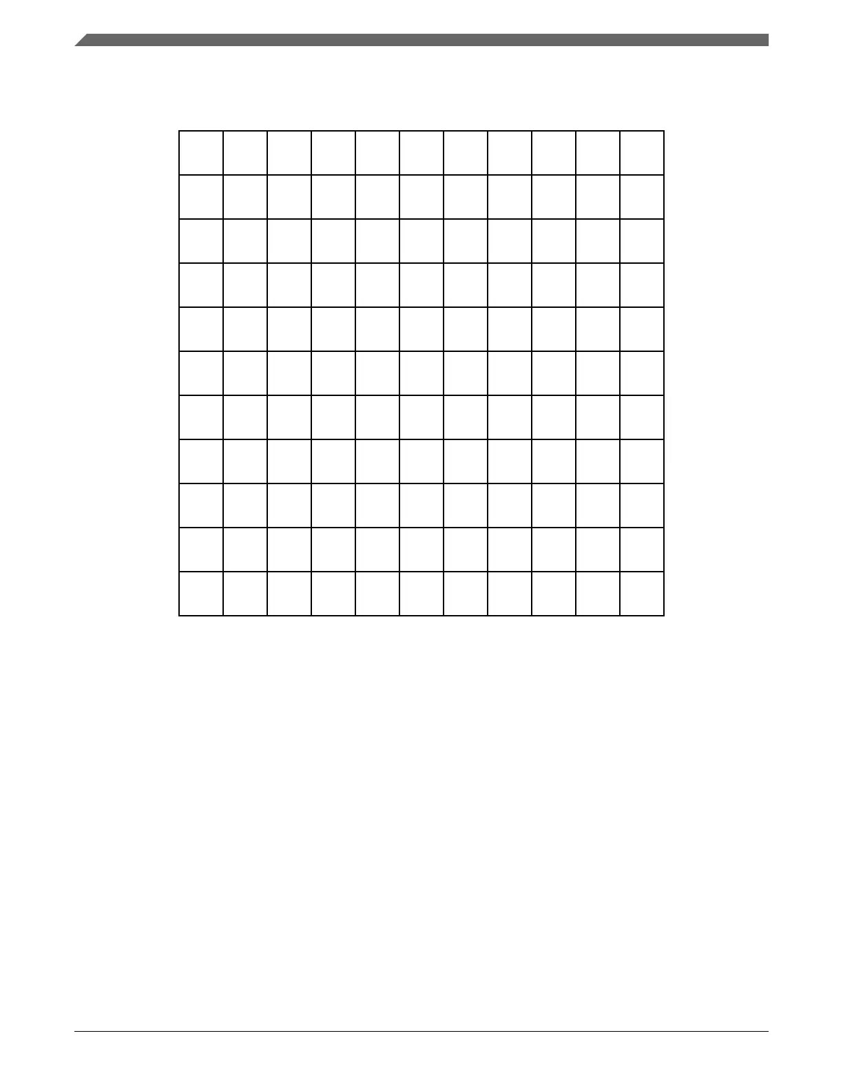
1
A PTD7
B PTD10
C PTD12
D PTD14
E PTD15
F USB0_DP
G VOUT33
H ADC0_DP1
J
ADC1_DP1/
ADC0_DP2
K
ADC0_DP0/
ADC1_DP3
1
L
ADC1_DP0/
ADC0_DP3
2
PTD5
PTD6/
LLWU_P15
PTD11
PTD13
PTE2/
LLWU_P1
USB0_DM
VREGIN
ADC0_DM1
ADC1_DM1/
ADC0_DM2
ADC0_DM0/
ADC1_DM3
2
ADC1_DM0/
ADC0_DM3
3
PTD4/
LLWU_P14
PTD3
PTD2/
LLWU_P13
PTD1
PTE1/
LLWU_P0
PTE6
VSS
ADC0_SE16/
CMP1_IN2/
ADC0_SE21
ADC1_SE16/
ADC0_SE22
NC
3
VREF_OUT/
CMP1_IN5/
CMP0_IN5/
ADC1_SE18
4
PTC19
PTC18
PTC17
PTD0/
LLWU_P12
PTE0/
CLKOUT32K
PTE3
PTE5
NC
PTA11
DAC1_OUT/
CMP0_IN4/
ADC1_SE23
4
XTAL32
5
PTC14
PTC15
PTC11/
LLWU_P11
PTC16
VDD
VDDA
VREFH
PTE24
PTE25
DAC0_OUT/
CMP1_IN3/
ADC0_SE23
5
EXTAL32
6
PTC13
PTC12
PTC10
PTC9
VDD
VSSA
VREFL
PTE26/
CLKOUT32K
PTA0
VBAT
6
VSS
7
PTC8
PTC7
PTC6/
LLWU_P10
PTC5/
LLWU_P9
VDD
VSS
VSS
PTE4/
LLWU_P2
PTA2
PTA5
7
RTC_
WAKEUP_B
8
PTC4/
LLWU_P8
PTC3/
LLWU_P7
PTC2
PTC1/
LLWU_P6
PTB23
PTB22
PTB3
PTA1
PTA4/
LLWU_P3
PTA12
8
PTA13/
LLWU_P4
9
PTD9
PTC0
PTB19
PTB18
PTB17
PTB21
PTB2
PTA3
PTA10
PTA14
9
PTA15
10
PTD8
PTB16
PTB11
PTB10
PTB9
PTB20
PTB1
PTA17
PTA16
VSS
10
VDD
11
ANC
BNC
CNC
DPTB8
EPTB7
FPTB6
G
PTB0/
LLWU_P5
HPTA29
JRESET_b
KPTA19
11
LPTA18
Figure 10-7. K22F 121 XFBGA pinout diagram (transparent top view)
10.4
Module Signal Description Tables
The following sections correlate the chip-level signal name with the signal name used in
the module's chapter. They also briefly describe the signal function and direction.
Module Signal Description Tables
K22F Sub-Family Reference Manual, Rev. 4, 08/2016
228 NXP Semiconductors

 Loading...