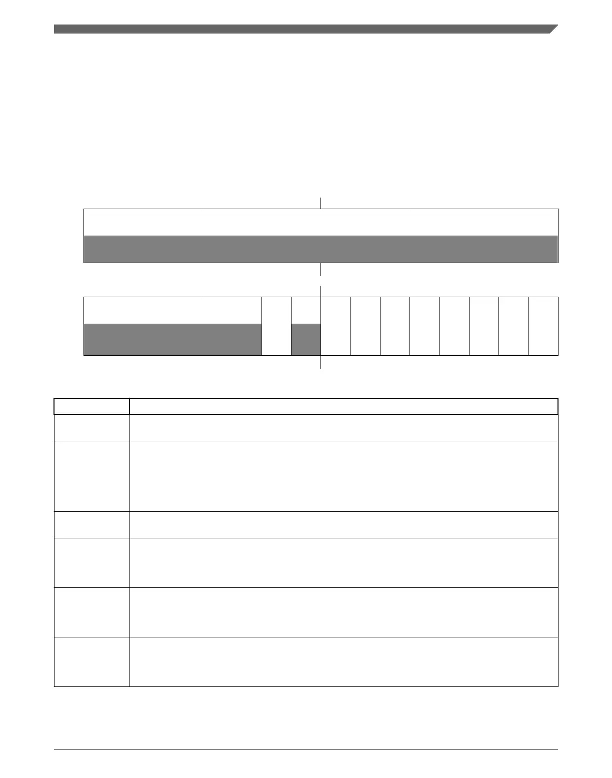
39.3.27 FTM PWM Load (FTMx_PWMLOAD)
Enables the loading of the MOD, CNTIN, C(n)V, and C(n+1)V registers with the values
of their write buffers when the FTM counter changes from the MOD register value to its
next value or when a channel (j) match occurs. A match occurs for the channel (j) when
FTM counter = C(j)V.
Address: Base address + 98h offset
Bit 31 30 29 28 27 26 25 24 23 22 21 20 19 18 17 16
R
0
W
Reset
0 0 0 0 0 0 0 0 0 0 0 0 0 0 0 0
Bit
15 14 13 12 11 10 9 8 7 6 5 4 3 2 1 0
R
0
LDOK
0
CH7SEL
CH6SEL
CH5SEL
CH4SEL
CH3SEL
CH2SEL
CH1SEL
CH0SEL
W
Reset
0 0 0 0 0 0 0 0 0 0 0 0 0 0 0 0
FTMx_PWMLOAD field descriptions
Field Description
31–10
Reserved
This field is reserved.
This read-only field is reserved and always has the value 0.
9
LDOK
Load Enable
Enables the loading of the MOD, CNTIN, and CV registers with the values of their write buffers.
0 Loading updated values is disabled.
1 Loading updated values is enabled.
8
Reserved
This field is reserved.
This read-only field is reserved and always has the value 0.
7
CH7SEL
Channel 7 Select
0 Do not include the channel in the matching process.
1 Include the channel in the matching process.
6
CH6SEL
Channel 6 Select
0 Do not include the channel in the matching process.
1 Include the channel in the matching process.
5
CH5SEL
Channel 5 Select
0 Do not include the channel in the matching process.
1 Include the channel in the matching process.
Table continues on the next page...
Chapter 39 FlexTimer Module (FTM)
K22F Sub-Family Reference Manual, Rev. 4, 08/2016
NXP Semiconductors 945

 Loading...