RNG_OR field descriptions (continued)
Field Description
0 Invalid data (if you read this field when it is 0 and SR[OREG_LVL] is 0, RNGA then
writes 1 to SR[ERRI], SR[ORU], and SR[LRS]; when the error interrupt is not masked
(CR[INTM]=0), RNGA also asserts an error interrupt request to the interrupt controller).
All other values Valid data (if you read this field when SR[OREG_LVL] is not 0, RNGA returns
RANDOUT, and then writes 0 to this field and to SR[OREG_LVL]).
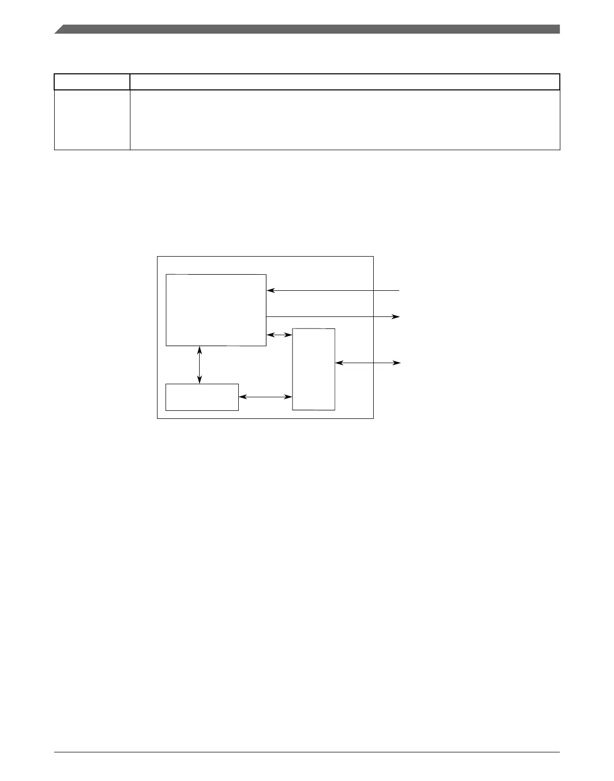
33.4 Functional description
This is a block diagram of RNGA.
Core engine/
control logic
Output (OR)
register
Internal bus
RNGA
Bus
interface
Internal
control
signals
Figure 33-1. RNGA block diagram
33.4.1
Output (OR) register
The Output (OR) register provides temporary storage for random data generated by the
core engine / control logic. The Status (SR) register allows the user to monitor the
presence of valid random data in OR through SR[OREG_LVL].
If the OR is read while containing valid random data (as signaled by SR[OREG_LVL] =
1), the valid data is returned, then OR and SR[OREG_LVL] are both cleared. If the user
reads from OR when it is empty, RNGA returns all zeros and, if the interrupt is enabled,
RNGA drives a request to the interrupt controller. Polling SR[OREG_LVL] is very
important to make sure random values are present before reading from OR.
Functional description
K22F Sub-Family Reference Manual, Rev. 4, 08/2016
758 NXP Semiconductors

 Loading...