MCG_C6 field descriptions
Field Description
7
LOLIE0
Loss of Lock Interrrupt Enable
Determines if an interrupt request is made following a loss of lock indication. This bit only has an effect
when LOLS 0 is set.
0 No interrupt request is generated on loss of lock.
1 Generate an interrupt request on loss of lock.
6
PLLS
PLL Select
Controls whether the PLL or FLL output is selected as the MCG source when CLKS[1:0]=00. If the PLLS
bit is cleared and PLLCLKEN 0 is not set, the PLL is disabled in all modes. If the PLLS is set, the FLL is
disabled in all modes.
0 FLL is selected.
1
PLL is selected (PRDIV 0 need to be programmed to the correct divider to generate a PLL reference
clock in the range of 2–4 MHz prior to setting the PLLS bit).
5
CME0
Clock Monitor Enable
Enables the loss of clock monitoring circuit for the OSC0 external reference mux select. The LOCRE0 bit
will determine if a interrupt or a reset request is generated following a loss of OSC0 indication. The CME0
bit must only be set to a logic 1 when the MCG is in an operational mode that uses the external clock
(FEE, FBE, PEE, PBE, or BLPE) . Whenever the CME0 bit is set to a logic 1, the value of the RANGE0
bits in the C2 register should not be changed. CME0 bit should be set to a logic 0 before the MCG enters
any Stop mode. Otherwise, a reset request may occur while in Stop mode. CME0 should also be set to a
logic 0 before entering VLPR or VLPW power modes if the MCG is in BLPE mode.
0 External clock monitor is disabled for OSC0.
1 External clock monitor is enabled for OSC0.
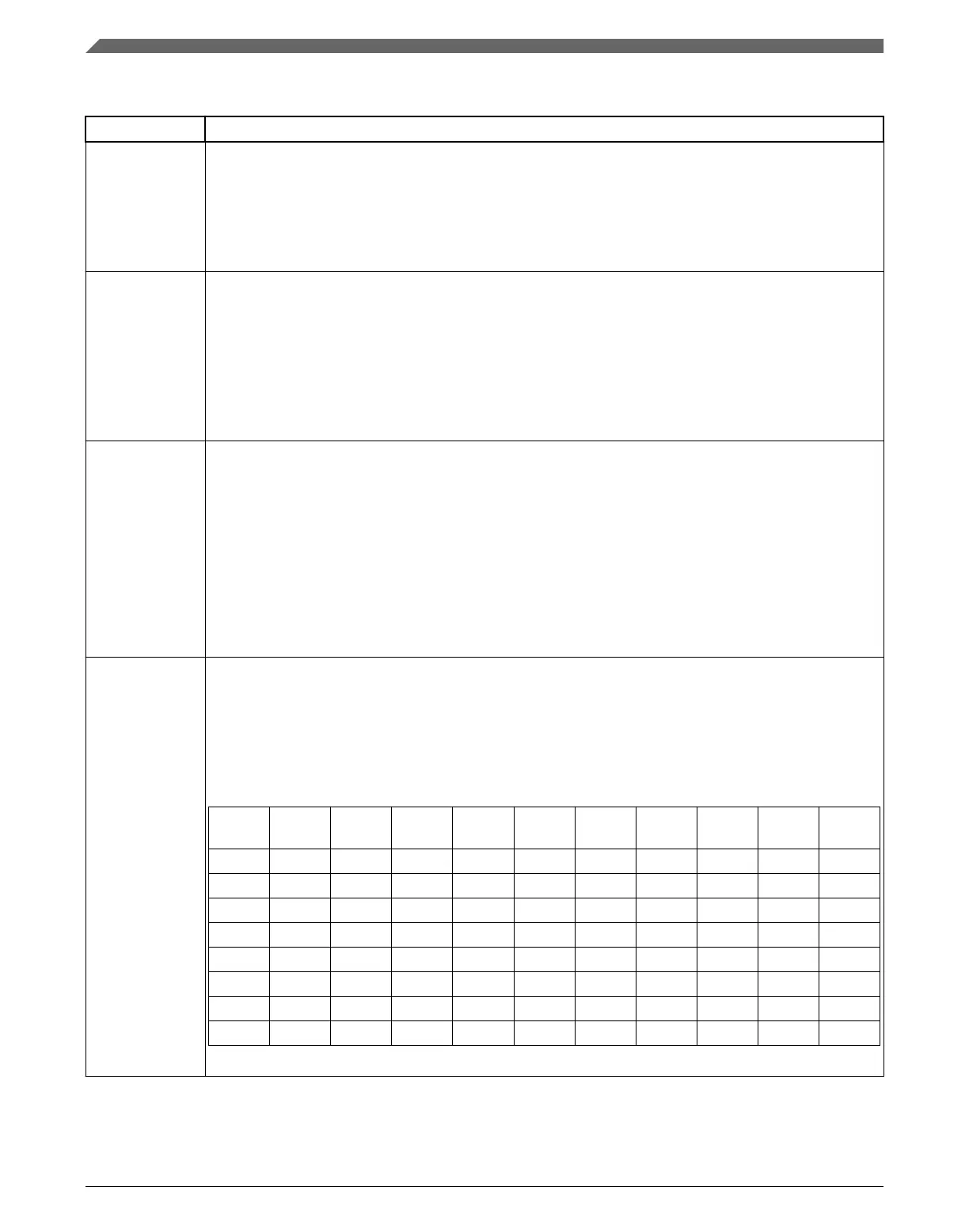
VDIV0 VCO 0 Divider
Selects the amount to divide the VCO output of the PLL. The VDIV 0 bits establish the multiplication factor
(M) applied to the reference clock frequency. After the PLL is enabled (by setting either PLLCLKEN 0 or
PLLS), the VDIV 0 value must not be changed when LOCK 0 is zero.
Table 25-2. PLL VCO Divide Factor
VDIV 0 Multiply
Factor
VDIV 0 Multiply
Factor
VDIV 0 Multiply
Factor
VDIV 0 Multiply
Factor
00000 24 01000 32 10000 40 11000 48
00001 25 01001 33 10001 41 11001 49
00010 26 01010 34 10010 42 11010 50
00011 27 01011 35 10011 43 11011 51
00100 28 01100 36 10100 44 11100 52
00101 29 01101 37 10101 45 11101 53
00110 30 01110 38 10110 46 11110 54
00111 31 01111 39 10111 47 11111 55
Memory Map/Register Definition
K22F Sub-Family Reference Manual, Rev. 4, 08/2016
550 NXP Semiconductors

 Loading...