3.8.1.2 PDB Module Interconnections
PDB trigger outputs Connection
Channel 0 triggers ADC0 trigger
Channel 1 triggers ADC1 trigger and synchronous input 1 of FTM0
DAC triggers DAC0 and DAC1 trigger
Pulse-out Pulse-out connected to each CMP module's sample/window
input to control sample operation
3.8.1.3 Back-to-back acknowledgement connections
Back-to-back operation enables the ADC conversions complete to trigger the next PDB
channel pre-trigger and trigger output.
In this MCU, PDB back-to-back operation acknowledgment connections are
implemented as follows:
• PDB channel 0 trigger/pre-trigger 0 acknowledgement input: ADC1SC1B_COCO
• PDB channel 0 trigger/pre-trigger 1 acknowledgement input: ADC0SC1A_COCO
• PDB channel 1 trigger/pre-trigger 0 acknowledgement input: ADC0SC1B_COCO
• PDB channel 1 trigger/pre-trigger 1 acknowledgement input: ADC1SC1A_COCO
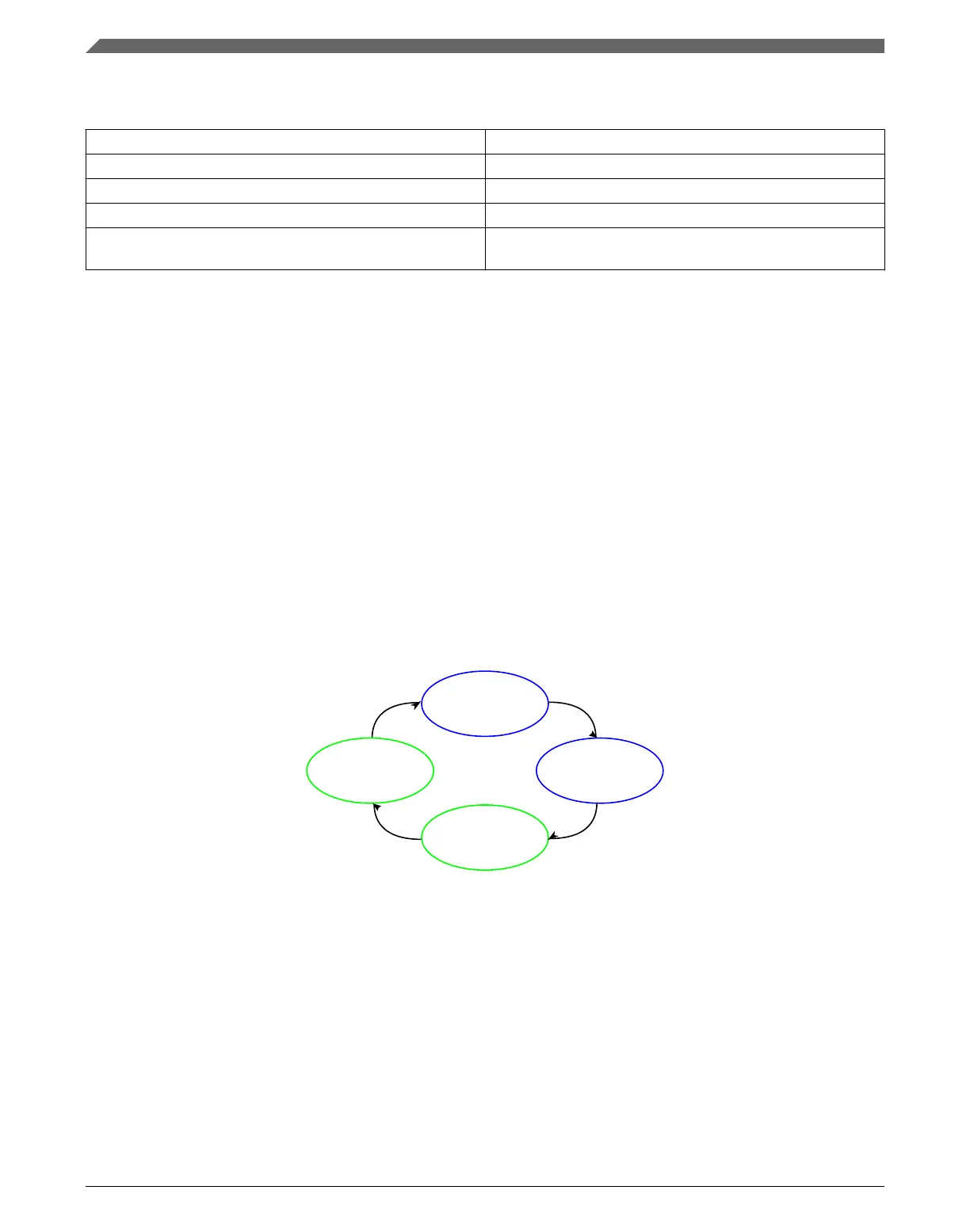
So, the back-to-back chain is connected as a ring:
Channel 0
pre-trigger 0
Channel 1
pre-trigger 0
Channel 0
pre-trigger 1
Channel 1
pre-trigger 1
Figure 3-37. PDB back-to-back chain
The application code can set the PDBx_CHnC1[BB] bits to configure the PDB pre-
triggers as a single chain or several chains.
3.8.1.4
PDB Interval Trigger Connections to DAC
In this MCU, PDB interval trigger connections to DAC are implemented as follows.
Timers
K22F Sub-Family Reference Manual, Rev. 4, 08/2016
110 NXP Semiconductors

 Loading...