PCSx
SCK
Master SIN
t
CSC =
PCS to SCK dela
t
ASC =
After SCK delay
SCK (CPOL = 0)
SCK (CPOL = 1)
Master SOUT
t
DT =
Delay after Transfer (minimum CS negation time)
t
CSC
t
ASC
t
CSC
t
DT
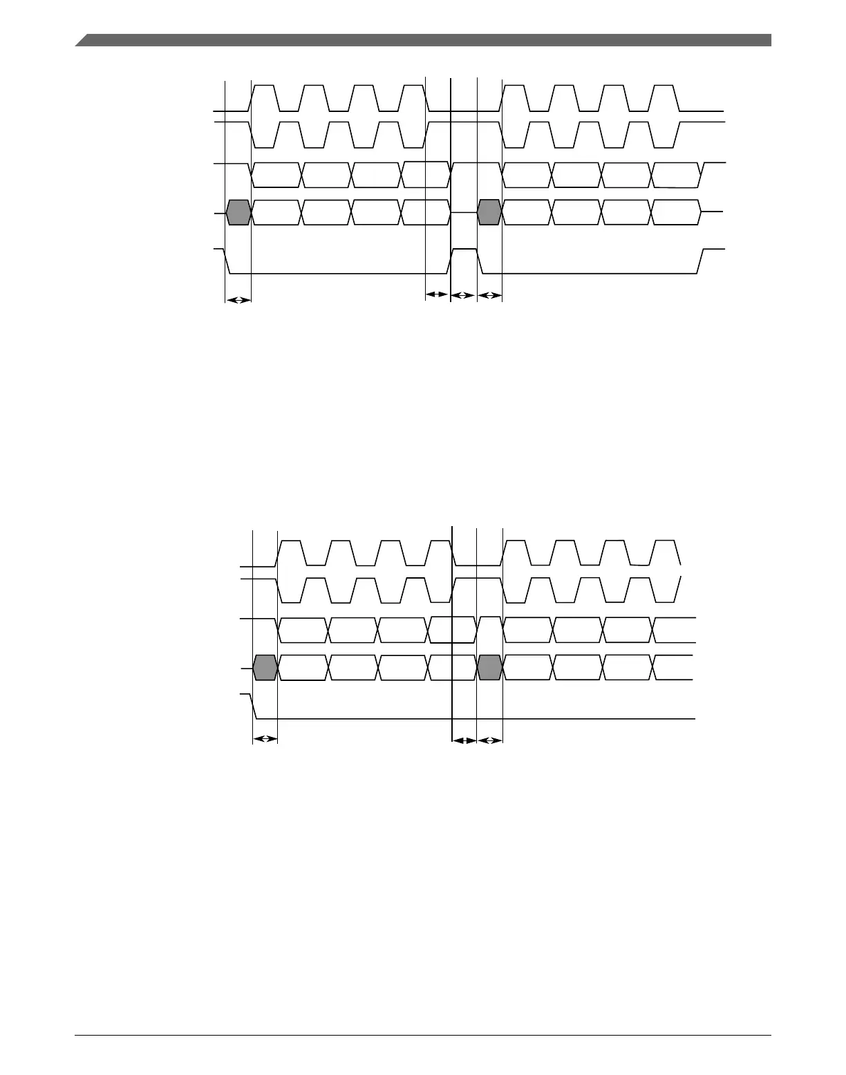
Figure 45-14. Example of non-continuous format (CPHA=1, CONT=0)
When the CONT bit = 1, the PCS signal remains asserted for the duration of the two
transfers. The Delay between Transfers (t
DT
) is not inserted between the transfers. The
following figure shows the timing diagram for two four-bit transfers with CPHA = 1 and
CONT = 1.
PCS
Master SIN
tCSC
=
P
C
S
to SCK del ay
t
ASC
=
After SCK delay
SCK (CPOL = 0)
SCK (CPOL = 1)
Master SOUT
t
CSC
t
ASC
t
CSC
Figure 45-15. Example of continuous transfer (CPHA=1, CONT=1)
When using the module with continuous selection follow these rules:
• All transmit commands must have the same PCSn bits programming.
• The CTARs, selected by transmit commands, must be programmed with the same
transfer attributes. Only FMSZ field can be programmed differently in these CTARs.
Functional description
K22F Sub-Family Reference Manual, Rev. 4, 08/2016
1168 NXP Semiconductors

 Loading...