It is recommended to keep the baud rate the same while using the Continuous SCK.
Switching clock polarity between frames while using Continuous SCK can cause errors
in the transfer. Continuous SCK operation is not guaranteed if the module is put into the
External Stop mode or Module Disable mode.
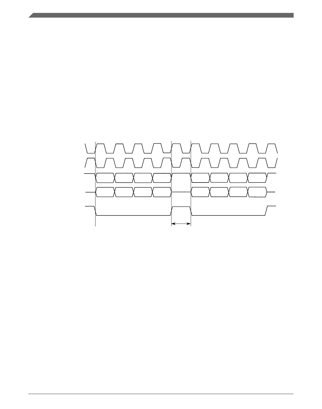
Enabling Continuous SCK disables the PCS to SCK delay and the Delay after Transfer
(t
DT
) is fixed to one SCK cycle. The following figure is the timing diagram for
Continuous SCK format with Continuous Selection disabled.
NOTE
In Continuous SCK mode, for the SPI transfer CTAR0 should
always be used, and the TX FIFO must be cleared using the
MCR[CLR_TXF] field before initiating transfer.
PCS
Master SIN
SCK (CPOL = 0)
SCK (CPOL = 1)
Master SOUT
t
DT
Figure 45-16. Continuous SCK Timing Diagram (CONT=0)
If the CONT bit in the TX FIFO entry is set, PCS remains asserted between the transfers.
Under certain conditions, SCK can continue with PCS asserted, but with no data being
shifted out of SOUT, that is, SOUT pulled high. This can cause the slave to receive
incorrect data. Those conditions include:
• Continuous SCK with CONT bit set, but no data in the TX FIFO.
• Continuous SCK with CONT bit set and entering Stopped state (refer to Start and
Stop of module transfers).
• Continuous SCK with CONT bit set and entering Stop mode or Module Disable
mode.
The following figure shows timing diagram for Continuous SCK format with Continuous
Selection enabled.
Functional description
K22F Sub-Family Reference Manual, Rev. 4, 08/2016
1170 NXP Semiconductors

 Loading...