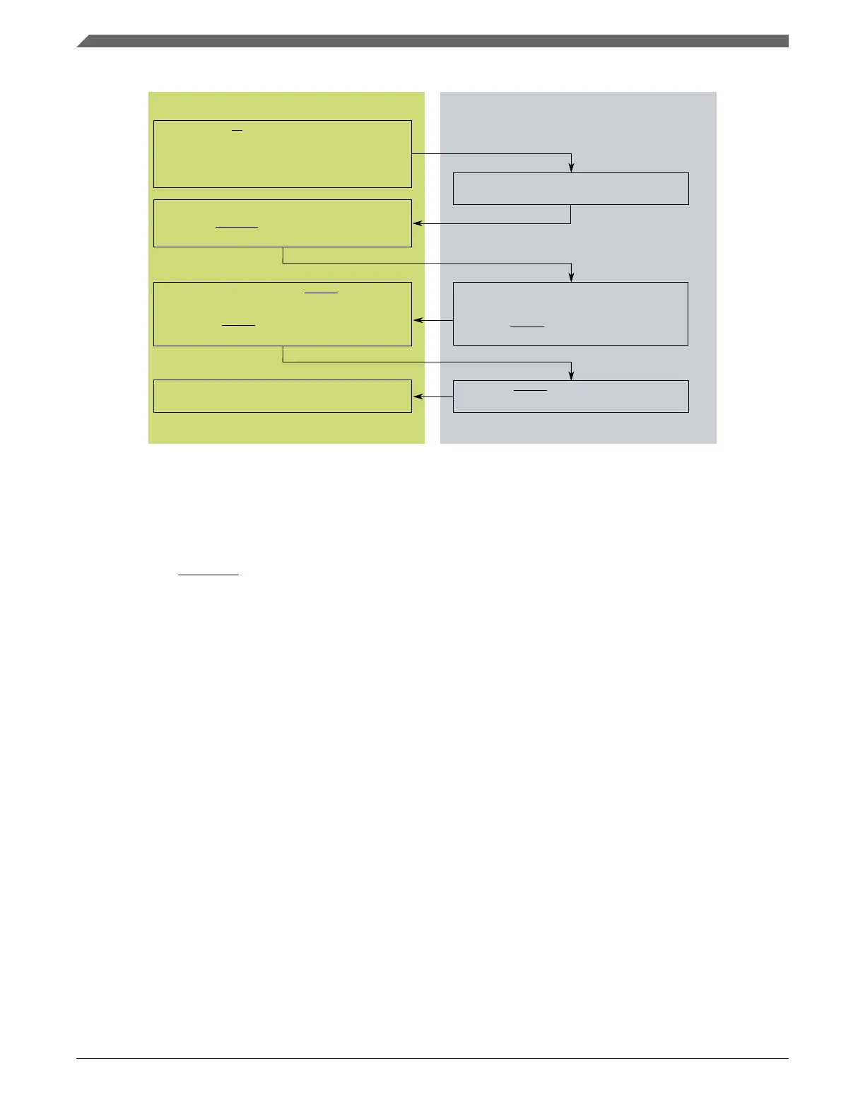
Decode address.
3. Assert FB_TA (external termination).
Negate FB_TA (external termination).
1. Set FB_R/W to read.
2. Assert FB_CSn.
(auto-acknowledge/internal termination).
2. Sample FB_TA low and latch data.
Start next cycle.
System
2. Place address on the external address signals.
2. Drive data on the external data signals.
1. Select the appropriate slave device.
3. Assert transfer start.
1. Negate transfer start.
1. FlexBus asserts internal FB_TA
Microcontroller
Figure 31-3. Read Cycle Flowchart
The read cycle timing diagram is shown in the following figure.
Note
FB_TA does not have to be driven by the external device for
internally-terminated bus cycles.
Note
The processor drives the data lines during the first clock cycle
of the transfer with the full 32-bit address. This may be ignored
by standard connected devices using non-multiplexed address
and data buses. However, some applications may find this
feature beneficial.
The address and data busses are muxed between the FlexBus
and another module. At the end of the read bus cycles the
address signals are indeterminate.
Functional description
K22F Sub-Family Reference Manual, Rev. 4, 08/2016
710 NXP Semiconductors

 Loading...