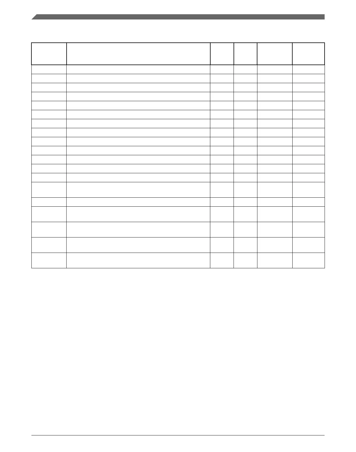
PDB memory map
Absolute
address
(hex)
Register name
Width
(in bits)
Access Reset value
Section/
page
4003_6000 Status and Control register (PDB0_SC) 32 R/W 0000_0000h 38.3.1/873
4003_6004 Modulus register (PDB0_MOD) 32 R/W 0000_FFFFh 38.3.2/876
4003_6008 Counter register (PDB0_CNT) 32 R 0000_0000h 38.3.3/876
4003_600C Interrupt Delay register (PDB0_IDLY) 32 R/W 0000_FFFFh 38.3.4/877
4003_6010 Channel n Control register 1 (PDB0_CH0C1) 32 R/W 0000_0000h 38.3.5/877
4003_6014 Channel n Status register (PDB0_CH0S) 32 R/W 0000_0000h 38.3.6/878
4003_6018 Channel n Delay 0 register (PDB0_CH0DLY0) 32 R/W 0000_0000h 38.3.7/879
4003_601C Channel n Delay 1 register (PDB0_CH0DLY1) 32 R/W 0000_0000h 38.3.8/880
4003_6038 Channel n Control register 1 (PDB0_CH1C1) 32 R/W 0000_0000h 38.3.5/877
4003_603C Channel n Status register (PDB0_CH1S) 32 R/W 0000_0000h 38.3.6/878
4003_6040 Channel n Delay 0 register (PDB0_CH1DLY0) 32 R/W 0000_0000h 38.3.7/879
4003_6044 Channel n Delay 1 register (PDB0_CH1DLY1) 32 R/W 0000_0000h 38.3.8/880
4003_6150 DAC Interval Trigger n Control register (PDB0_DACINTC0) 32 R/W 0000_0000h 38.3.9/880
4003_6154 DAC Interval n register (PDB0_DACINT0) 32 R/W 0000_0000h
38.3.10/
881
4003_6158 DAC Interval Trigger n Control register (PDB0_DACINTC1) 32 R/W 0000_0000h 38.3.9/880
4003_615C DAC Interval n register (PDB0_DACINT1) 32 R/W 0000_0000h
38.3.10/
881
4003_6190 Pulse-Out n Enable register (PDB0_POEN) 32 R/W 0000_0000h
38.3.11/
882
4003_6194 Pulse-Out n Delay register (PDB0_PO0DLY) 32 R/W 0000_0000h
38.3.12/
882
4003_6198 Pulse-Out n Delay register (PDB0_PO1DLY) 32 R/W 0000_0000h
38.3.12/
882
Memory map and register definition
K22F Sub-Family Reference Manual, Rev. 4, 08/2016
872 NXP Semiconductors

 Loading...