UM10360 All information provided in this document is subject to legal disclaimers. © NXP B.V. 2013. All rights reserved.
User manual Rev. 3 — 19 December 2013 476 of 841
NXP Semiconductors
UM10360
Chapter 20: LPC176x/5x I2S
20.4 Pin descriptions
Table 403. Pin descriptions
Pin Name Type Description
I2SRX_CLK Input/
Output
Receive Clock. A clock signal used to synchronize the transfer of data on the receive channel. It is
driven by the master and received by the slave. Corresponds to the signal SCK in the I
2
S-bus
specification.
I2SRX_WS Input/
Output
Receive Word Select. Selects the channel from which data is to be received. It is driven by the
master and received by the slave. Corresponds to the signal WS in the I
2
S-bus specification.
WS = 0 indicates that data is being received by channel 1 (left channel).
WS = 1 indicates that data is being received by channel 2 (right channel).
I2SRX_SDA Input/
Output
Receive Data. Serial data, received MSB first. It is driven by the transmitter and read by the
receiver. Corresponds to the signal SD in the I
2
S-bus specification.
RX_MCLK Output Optional master clock output for the
I
2
S receive function.
I2STX_CLK Input/
Output
Transmit Clock. A clock signal used to synchronize the transfer of data on the transmit channel. It
is driven by the master and received by the slave. Corresponds to the signal SCK in the I
2
S-bus
specification.
I2STX_WS Input/
Output
Transmit Word Select. Selects the channel to which data is being sent. It is driven by the master
and received by the slave. Corresponds to the signal WS in the I
2
S-bus specification.
WS = 0 indicates that data is being sent to channel 1 (left channel).
WS = 1 indicates that data is being sent to channel 2 (right channel).
I2STX_SDA Input/
Output
Transmit Data. Serial data, sent MSB first. It is driven by the transmitter and read by the receiver.
Corresponds to the signal SD in the I
2
S-bus specification.
TX_MCLK Output Optional master clock output for the
I
2
S transmit function.
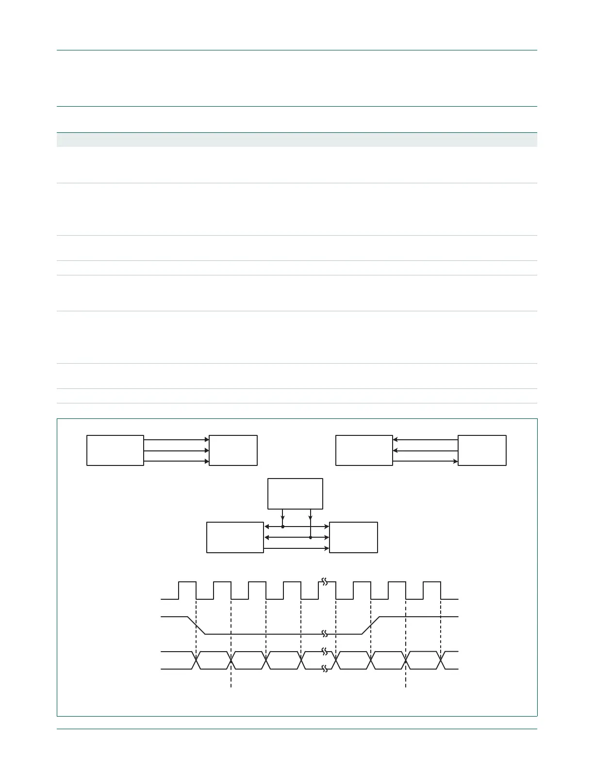
Fig 100. Simple I
2
S configurations and bus timing
TRANSMITTER
(MASTER)
CONTROLLER
(MASTER)
TRANSMITTER
(SLAVE)
RECEIVER
(MASTER)
SCK: serial clock
WS: word select
SD: serial data
TRANSMITTER
(SLAVE)
RECEIVER
(SLAVE)
SCK
WS
SD
SCK
WS
SD
MSB LSB MSB
word n
left channel
word n+1
right channel
word n-1
right channel
RECEIVER
(SLAVE)
SCK: serial clock
WS: word select
SD: serial data

 Loading...


