UM10360 All information provided in this document is subject to legal disclaimers. © NXP B.V. 2013. All rights reserved.
User manual Rev. 3 — 19 December 2013 30 of 841
4.1 Summary of clocking and power control functions
This section describes the generation of the various clocks needed by the LPC176x/5x
and options of clock source selection, as well as power control and wake-up from reduced
power modes. Functions described in the following subsections include:
• Oscillators
• Clock source selection
• PLLs
• Clock dividers
• APB dividers
• Power control
• Wake-up timer
• External clock output
UM10360
Chapter 4: LPC176x/5x Clocking and power control
Rev. 3 — 19 December 2013 User manual
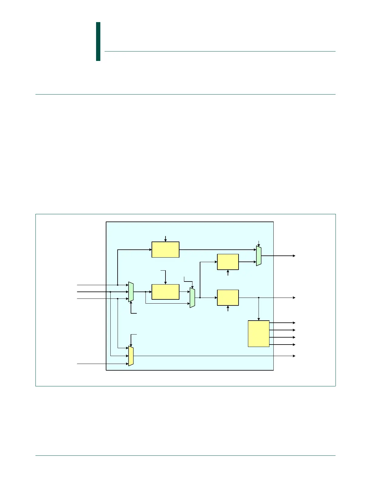
Fig 7. Clock generation for the LPC176x/5x
`
USB
Clock
Divider
osc_clk
irc_osc
system clock select
CLKSRCSEL[1:0]
USB PLL settings
(PLL1...)
USB clock divider setting
USBCLKCFG[3:0]
PCLK_WDT
Peripheral
Clock
Divider
wd_clk
usb_clk
pclk1
pclk8
pclk4
pclk2
USB PLL
(PLL1)
main PLL
settings
(PLL0...)
USB PLL
select
(PLL1CON)
Main PLL
(PLL0)
CPU
Clock
Divider
pllclk
CPU PLL
select
(PLL0CON)
cclk
watchdog clock select
WDCLKSEL[1:0]
rtc_clk
CPU clock divider setting
CCLKCFG[7:0]
sysclk

 Loading...


