UM10360 All information provided in this document is subject to legal disclaimers. © NXP B.V. 2013. All rights reserved.
User manual Rev. 3 — 20 December 2013 739 of 841
NXP Semiconductors
UM10360
Chapter 34: Appendix: Cortex-M3 user guide
‘<‘ means that accesses are observed in program order, that is, A1 is always observed
before A2.
34.3.2.3 Behavior of memory accesses
The behavior of accesses to each region in the memory map is:
[1] See Section 34.3.2.1 for more information.
The Code, SRAM, and external RAM regions can hold programs. However, the most
efficient access to programs is from the Code region. This is because the processor has
separate buses that enable instruction fetches and data accesses to occur
simultaneously.
The MPU can override the default memory access behavior described in this section. For
more information, see Section 34.4.5 “
Memory protection unit”.
34.3.2.4 Software ordering of memory accesses
The order of instructions in the program flow does not always guarantee the order of the
corresponding memory transactions. This is because:
• the processor can reorder some memory accesses to improve efficiency, providing
this does not affect the behavior of the instruction sequence.
• the processor has multiple bus interfaces
• memory or devices in the memory map have different wait states
• some memory accesses are buffered or speculative.
Section 34.3.2.2
describes the cases where the memory system guarantees the order of
memory accesses. Otherwise, if the order of memory accesses is critical, software must
include memory barrier instructions to force that ordering. The processor provides the
following memory barrier instructions:
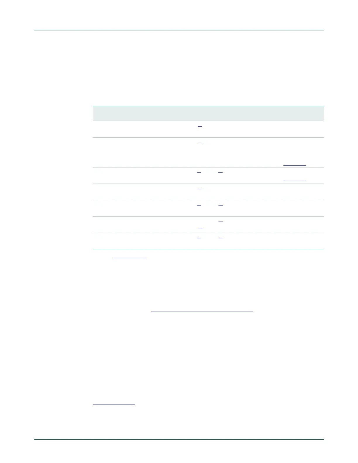
Table 635. Memory access behavior
Address
range
Memory
region
Memory
type
XN Description
0x00000000
-
0x1FFFFFFF
Code Normal
[1]
- Executable region for program code.
You can also put data here.
0x20000000
-
0x3FFFFFFF
SRAM Normal
[1]
- Executable region for data. You can
also put code here.
This region includes bit band and bit
band alias areas, see Table 636
.
0x40000000
-
0x5FFFFFFF
Peripheral Device
[1]
XN
[1]
This region includes bit band and bit
band alias areas, see Table 637
.
0x60000000
-
0x9FFFFFFF
External
RAM
Normal
[1]
- Executable region for data.
0xA0000000
-
0xDFFFFFFF
External
device
Device
[1]
XN
[1]
External Device memory
0xE0000000
-
0xE00FFFFF
Private Peripheral
Bus
Strongly-
ordered
[1]
XN
[1]
This region includes the NVIC, System
timer, and system control block.
0xE0100000
-
0xFFFFFFFF
Vendor-
specific device
Device
[1]
XN
[1]
Not used for NXP devices.

 Loading...


