UM10360 All information provided in this document is subject to legal disclaimers. © NXP B.V. 2013. All rights reserved.
User manual Rev. 3 — 19 December 2013 144 of 841
NXP Semiconductors
UM10360
Chapter 10: LPC176x/5x Ethernet
– Over-length frame support for both transmit and receive allows any length frames.
– Promiscuous receive mode.
– Automatic collision backoff and frame retransmission.
– Includes power management by clock switching.
– Wake-on-LAN power management support allows system wake-up: using the
receive filters or a magic frame detection filter.
• Physical interface:
– Attachment of external PHY chip through a standard Reduced MII (RMII) interface.
– PHY register access is available via the Media Independent Interface Management
(MIIM) interface.
10.4 Architecture and operation
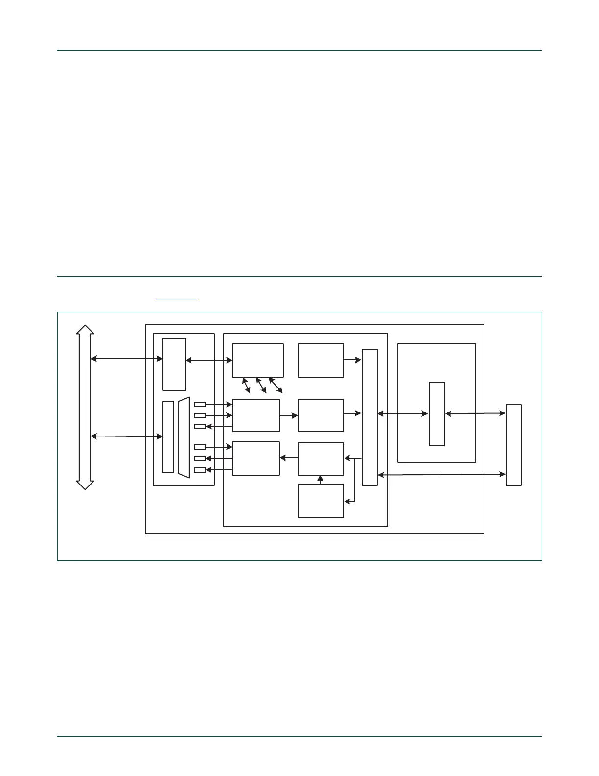
Figure 17 shows the internal architecture of the Ethernet block.
The block diagram for the Ethernet block consists of:
• The host registers module containing the registers in the software view and handling
AHB accesses to the Ethernet block. The host registers connect to the transmit and
receive data path as well as the MAC.
• The DMA to AHB interface. This provides an AHB master connection that allows the
Ethernet block to access on-chip SRAM for reading of descriptors, writing of status,
and reading and writing data buffers.
• The Ethernet MAC, which interfaces to the off-chip PHY via an RMII interface.
• The transmit data path, including:
Fig 17. Ethernet block diagram
register
interface (AHB
slave)
DMA interface
(AHB master)
BUS INTERFACE
RECEIVE
DMA
TRANSMIT
DMA
RECEIVE
BUFFER
RECEIVE
FILTER
TRANSMIT
RETRY
TRANSMIT
FLOW
CONTROL
ETHERNET MAC
RMII ADAPTER
RMII
MIIM
HOST
REGISTERS
AHB BUS
ETHERNET
BLOCK
ETHE RNET PHY
BUS
INTERFACE

 Loading...


