UM10360 All information provided in this document is subject to legal disclaimers. © NXP B.V. 2013. All rights reserved.
User manual Rev. 3 — 19 December 2013 588 of 841
NXP Semiconductors
UM10360
Chapter 31: LPC176x/5x General Purpose DMA (GPDMA)
• Big-endian and little-endian support. The DMA Controller defaults to little-endian
mode on reset.
• An interrupt to the processor can be generated on a DMA completion or when a DMA
error has occurred.
• Raw interrupt status. The DMA error and DMA count raw interrupt status can be read
prior to masking.
• DMA can operate in Sleep mode. (Note that in Sleep mode the GPDMA cannot
access the flash memory).
31.4 Functional description
This section describes the major functional blocks of the DMA Controller.
31.4.1 DMA controller functional description
The DMA Controller enables peripheral-to-memory, memory-to-peripheral,
peripheral-to-peripheral, and memory-to-memory transactions. Each DMA stream
provides unidirectional serial DMA transfers for a single source and destination. For
example, a bidirectional port requires one stream for transmit and one for receive. The
source and destination areas can each be either a memory region or a peripheral, and
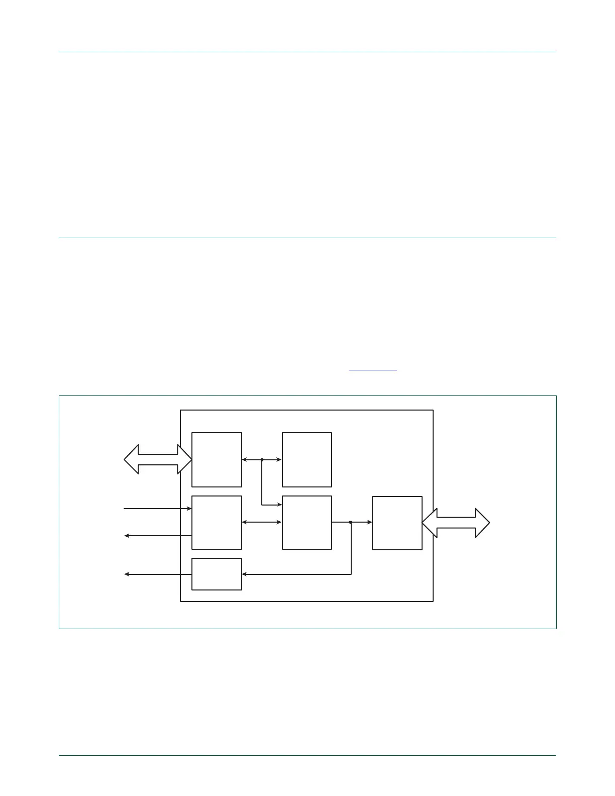
can be accessed through the AHB master. Figure 134
shows a block diagram of the DMA
Controller.
The functions of the DMA Controller are described in the following sections.
31.4.1.1 AHB slave interface
All transactions to DMA Controller registers on the AHB slave interface are 32 bits wide.
8-bit and 16-bit accesses are not supported and will result in an exception.
Fig 134. DMA controller block diagram
GPDMA
AHB SLAVE
INTERFACE
CONTROL
LOGIC AND
REGISTERS
DMA
REQUEST
AND
RESPONSE
INTERFACE
CHANNEL
LOGIC AND
REGISTERS
INTERRUPT
REQUEST
DMA
requests
DMA
responses
DMA
Interrupts
AHB BUS
AHB
MASTER
INTERFACE
AHB BUS

 Loading...


