UM10360 All information provided in this document is subject to legal disclaimers. © NXP B.V. 2013. All rights reserved.
User manual Rev. 3 — 19 December 2013 120 of 841
NXP Semiconductors
UM10360
Chapter 8: LPC176x/5x Pin connect block
8.5.21 I
2
C Pin Configuration register (I2CPADCFG - 0x4002 C07C)
The I2CPADCFG register allows configuration of the I
2
C pins for the I2C0 interface only, in
order to support various I
2
C-bus operating modes. For use in standard or Fast Mode I
2
C,
the 4 bits in I2CPADCFG should be 0, the default value for this register. For Fast Mode
Plus, the SDADRV0 and SCLDRV0 bits should be 1. For non-I
2
C use of these pins, it may
be desirable to turn off I
2
C filtering and slew rate control by setting SDAI2C0 and SCLI2C0
to 1. See Table 99
below.
28 P4.28OD Port 4 pin 28 open drain mode control. 0
0 P4.28 pin is in the normal (not open drain) mode.
1 P4.28 pin is in the open drain mode.
29 P4.28OD Port 4 pin 29 open drain mode control, see P4.28OD 0
31:30 - Reserved. NA
Table 98. Open Drain Pin Mode select register 4 (PINMODE_OD4 - address 0x4002 C078) bit
description …continued
PINMODE
_OD4
Symbol Value Description Reset
value
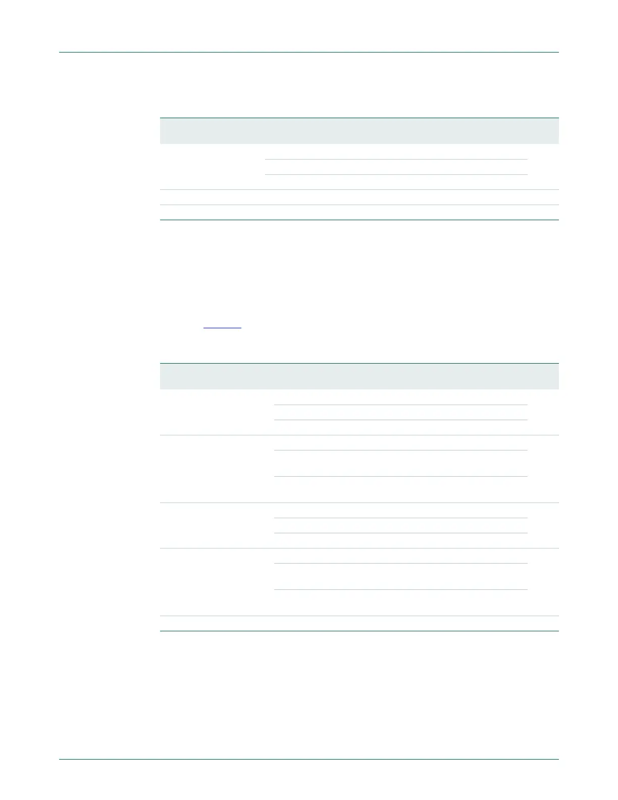
Table 99. I
2
C Pin Configuration register (I2CPADCFG - address 0x4002 C07C) bit
description
I2CPADCFG Symbol Value Description Reset
value
0 SDADRV0 Drive mode control for the SDA0 pin, P0.27. 0
0 The SDA0 pin is in the standard drive mode.
1 The SDA0 pin is in Fast Mode Plus drive mode.
1 SDAI2C0
I
2
C mode control for the SDA0 pin, P0.27. 0
0 The SDA0 pin has
I
2
C glitch filtering and slew rate
control enabled.
1 The SDA0 pin has
I
2
C glitch filtering and slew rate
control disabled.
2 SCLDRV0 Drive mode control for the SCL0 pin, P0.28. 0
0 The SCL0 pin is in the standard drive mode.
1 The SCL0 pin is in Fast Mode Plus drive mode.
3 SCLI2C0
I
2
C mode control for the SCL0 pin, P0.28. 0
0 The SCL0 pin has
I
2
C glitch filtering and slew rate
control enabled.
1 The SCL0 pin has
I
2
C glitch filtering and slew rate
control disabled.
31:4 - Reserved. NA

 Loading...


