UM10360 All information provided in this document is subject to legal disclaimers. © NXP B.V. 2013. All rights reserved.
User manual Rev. 3 — 19 December 2013 436 of 841
NXP Semiconductors
UM10360
Chapter 19: LPC176x/5x I2C0/1/2
19.7.2 Address Registers, I2ADR0 to I2ADR3
These registers may be loaded with the 7-bit slave address (7 most significant bits) to
which the I
2
C block will respond when programmed as a slave transmitter or receiver. The
LSB (GC) is used to enable General Call address (0x00) recognition. When multiple slave
addresses are enabled, the actual address received may be read from the I2DAT register
at the state where the “own slave address” has just been received.
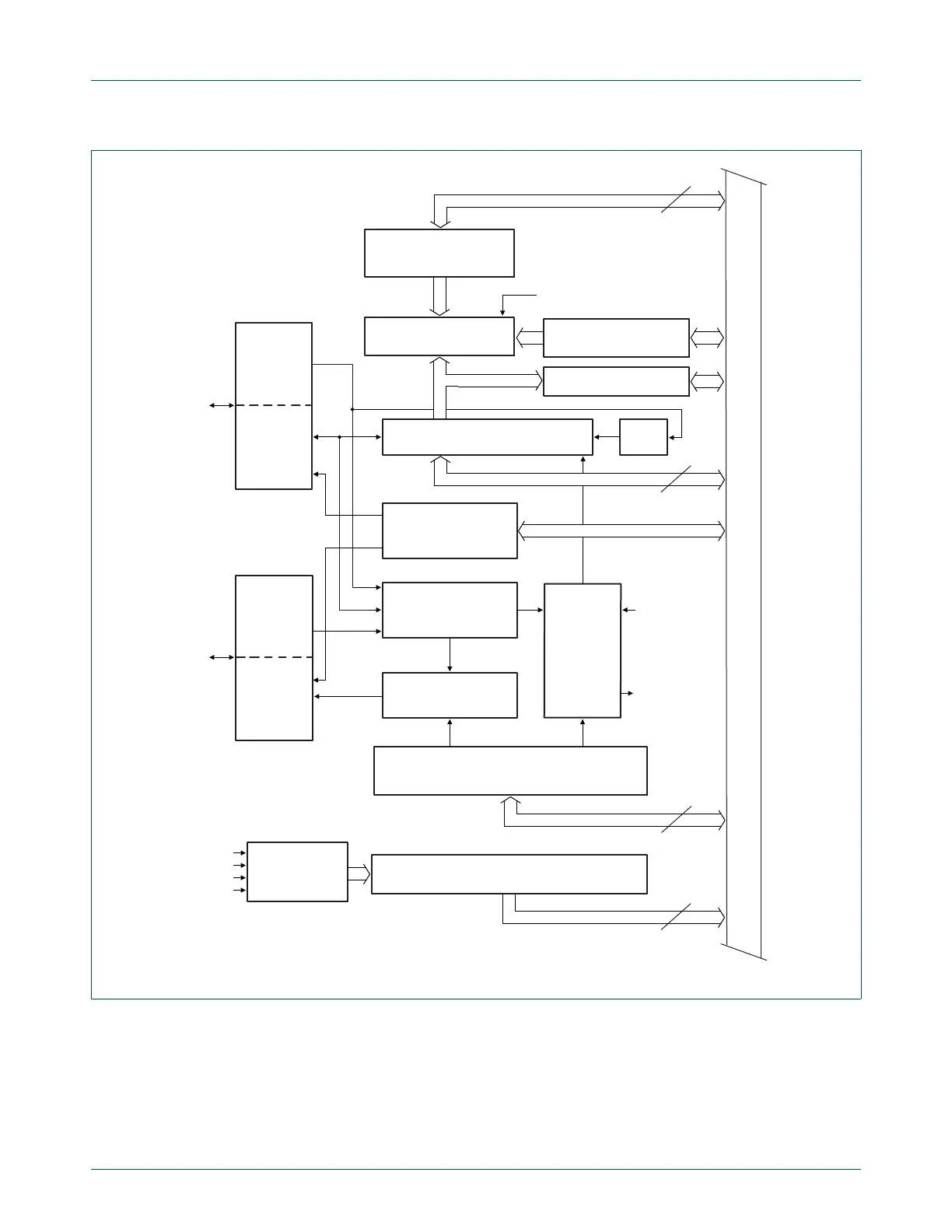
Fig 90. I
2
C serial interface block diagram
APB BUS
STATUS REGISTER
I2CnSTAT
CONTROL REGISTER and
SCL DUTY CYLE REGISTERS
I2CnCONSET, I2CnCONCLR, I2CnSCLH, I2CnSCLL
ADDRESS REGISTERS
MASK and COMPARE
SHIFT REGISTER
I2CnDAT
ACK
BIT COUNTER/
ARBITRATION and
MONITOR MODE
REGISTER
I2CnMMCTRL
SYNC LOGIC
SERIAL CLOCK
GENERATOR
TIMING and
CONTROL
LOGIC
STATUS
DECODER
status
bus
interrupt
PCLK
INPUT
FILTER
OUTPUT
STAGE
SCL
INPUT
FILTER
OUTPUT
STAGE
SDA
I2CnADDR0 to I2CnADDR3
MASK REGISTERS
I2CnMASK0 to I2CnMASK3
I2CnDATABUFFER
MATCHALL
I2CnMMCTRL[3]
8
8
8
16

 Loading...


