UM10360 All information provided in this document is subject to legal disclaimers. © NXP B.V. 2013. All rights reserved.
User manual Rev. 3 — 19 December 2013 108 of 841
NXP Semiconductors
UM10360
Chapter 8: LPC176x/5x Pin connect block
8.5 Register description
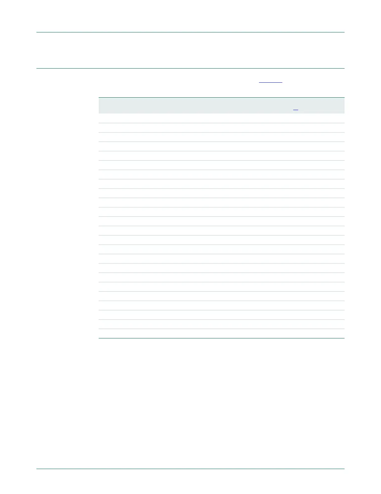
The Pin Control Module contains 11 registers as shown in Table 78 below.
[1] Reset Value reflects the data stored in used bits only. It does not include reserved bits content.
Pin control module register reset values
On external reset, watchdog reset, power-on-reset (POR), and BOD reset, all registers in
this module are reset to '0'.
Table 78. Pin Connect Block Register Map
Name Description Access Reset
Value
[1]
Address
PINSEL0 Pin function select register 0. R/W 0 0x4002 C000
PINSEL1 Pin function select register 1. R/W 0 0x4002 C004
PINSEL2 Pin function select register 2. R/W 0 0x4002 C008
PINSEL3 Pin function select register 3. R/W 0 0x4002 C00C
PINSEL4 Pin function select register 4 R/W 0 0x4002 C010
PINSEL7 Pin function select register 7 R/W 0 0x4002 C01C
PINSEL8 Pin function select register 8 R/W 0 0x4002 C020
PINSEL9 Pin function select register 9 R/W 0 0x4002 C024
PINSEL10 Pin function select register 10 R/W 0 0x4002 C028
PINMODE0 Pin mode select register 0 R/W 0 0x4002 C040
PINMODE1 Pin mode select register 1 R/W 0 0x4002 C044
PINMODE2 Pin mode select register 2 R/W 0 0x4002 C048
PINMODE3 Pin mode select register 3. R/W 0 0x4002 C04C
PINMODE4 Pin mode select register 4 R/W 0 0x4002 C050
PINMODE5 Pin mode select register 5 R/W 0 0x4002 C054
PINMODE6 Pin mode select register 6 R/W 0 0x4002 C058
PINMODE7 Pin mode select register 7 R/W 0 0x4002 C05C
PINMODE9 Pin mode select register 9 R/W 0 0x4002 C064
PINMODE_OD0 Open drain mode control register 0 R/W 0 0x4002 C068
PINMODE_OD1 Open drain mode control register 1 R/W 0 0x4002 C06C
PINMODE_OD2 Open drain mode control register 2 R/W 0 0x4002 C070
PINMODE_OD3 Open drain mode control register 3 R/W 0 0x4002 C074
PINMODE_OD4 Open drain mode control register 4 R/W 0 0x4002 C078
I2CPADCFG I
2
C Pin Configuration register R/W 0 0x4002 C07C

 Loading...


