UM10360 All information provided in this document is subject to legal disclaimers. © NXP B.V. 2013. All rights reserved.
User manual Rev. 3 — 19 December 2013 111 of 841
NXP Semiconductors
UM10360
Chapter 8: LPC176x/5x Pin connect block
[1] Not available on 80-pin package.
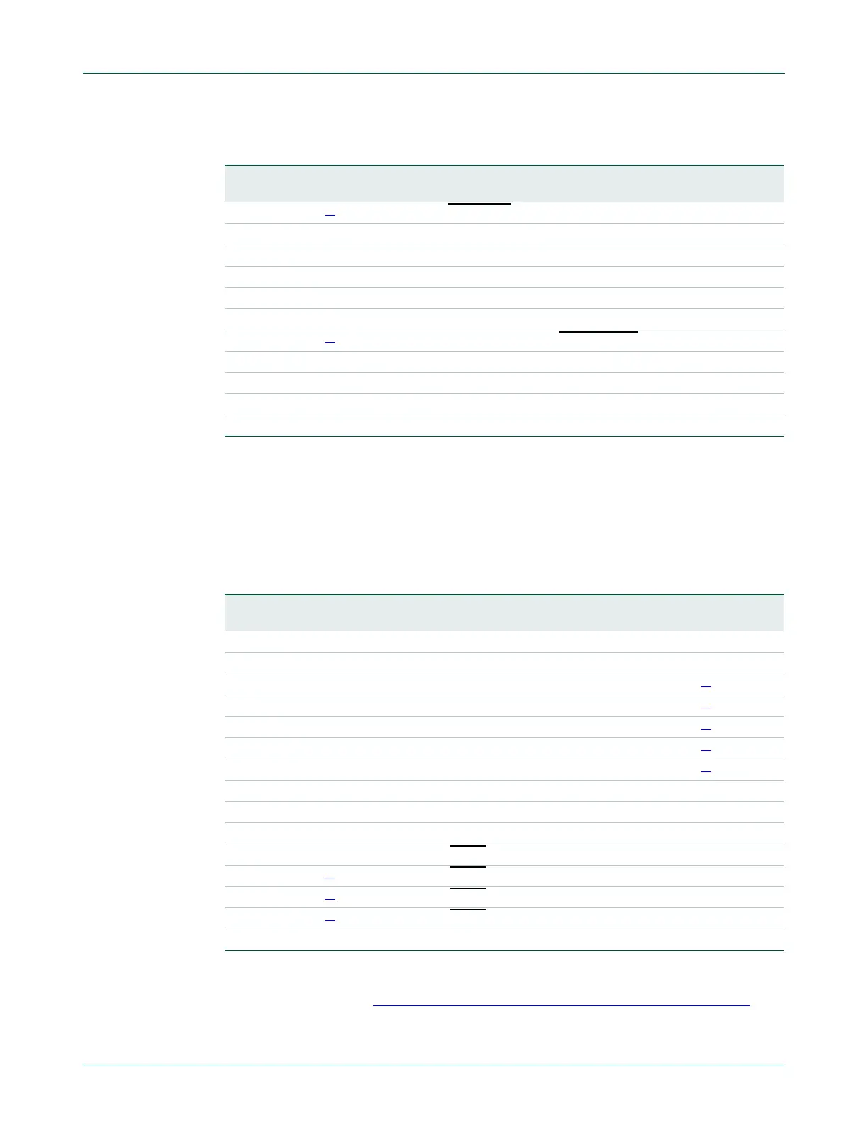
8.5.5 Pin Function Select Register 4 (PINSEL4 - 0x4002 C010)
The PINSEL4 register controls the functions of the lower half of Port 2. The direction
control bit in the FIO2DIR register is effective only when the GPIO function is selected for
a pin. For other functions, direction is controlled automatically.
[1] Not available on 80-pin package.
[2] These pins support a debug trace function when selected via a development tool or by writing to the
PINSEL10 register. See Section 8.5.8 “
Pin Function Select Register 10 (PINSEL10 - 0x4002 C028)” for
details.
11:10 P1.21
[1]
GPIO Port 1.21 MCABORT PWM1.3 SSEL0 00
13:12 P1.22 GPIO Port 1.22 MCOB0 USB_PWRD MAT1.0 00
15:14 P1.23 GPIO Port 1.23 MCI1 PWM1.4 MISO0 00
17:16 P1.24 GPIO Port 1.24 MCI2 PWM1.5 MOSI0 00
19:18 P1.25 GPIO Port 1.25 MCOA1 Reserved MAT1.1 00
21:20 P1.26 GPIO Port 1.26 MCOB1 PWM1.6 CAP0.0 00
23:22 P1.27
[1]
GPIO Port 1.27 CLKOUT USB_OVRCR CAP0.1 00
25:24 P1.28 GPIO Port 1.28 MCOA2 PCAP1.0 MAT0.0 00
27:26 P1.29 GPIO Port 1.29 MCOB2 PCAP1.1 MAT0.1 00
29:28 P1.30 GPIO Port 1.30 Reserved V
BUS
AD0.4 00
31:30 P1.31 GPIO Port 1.31 Reserved SCK1 AD0.5 00
Table 82. Pin function select register 3 (PINSEL3 - address 0x4002 C00C) bit
description …continued
PINSEL3 Pin
name
Function when
00
Function when
01
Function
when 10
Function
when 11
Reset
value
Table 83. Pin function select register 4 (PINSEL4 - address 0x4002 C010) bit description
PINSEL4 Pin
name
Function when
00
Function when 01 Function
when 10
Function when
11
Reset
value
1:0 P2.0 GPIO Port 2.0 PWM1.1 TXD1 Reserved 00
3:2 P2.1 GPIO Port 2.1 PWM1.2 RXD1 Reserved 00
5:4 P2.2 GPIO Port 2.2 PWM1.3 CTS1 Reserved
[2]
00
7:6 P2.3 GPIO Port 2.3 PWM1.4 DCD1 Reserved
[2]
00
9:8 P2.4 GPIO Port 2.4 PWM1.5 DSR1 Reserved
[2]
00
11:10 P2.5 GPIO Port 2.5 PWM1.6 DTR1 Reserved
[2]
00
13:12 P2.6 GPIO Port 2.6 PCAP1.0 RI1 Reserved
[2]
00
15:14 P2.7 GPIO Port 2.7 RD2 RTS1 Reserved 00
17:16 P2.8 GPIO Port 2.8 TD2 TXD2 ENET_MDC 00
19:18 P2.9 GPIO Port 2.9 USB_CONNECT RXD2 ENET_MDIO 00
21:20 P2.10 GPIO Port 2.10 EINT0
NMI Reserved 00
23:22 P2.11
[1]
GPIO Port 2.11 EINT1 Reserved I2STX_CLK 00
25:24 P2.12
[1]
GPIO Port 2.12 EINT2 Reserved I2STX_WS 00
27:26 P2.13
[1]
GPIO Port 2.13 EINT3 Reserved I2STX_SDA 00
31:28 - Reserved Reserved Reserved Reserved 0

 Loading...


