UM10360 All information provided in this document is subject to legal disclaimers. © NXP B.V. 2013. All rights reserved.
User manual Rev. 3 — 19 December 2013 275 of 841
NXP Semiconductors
UM10360
Chapter 13: LPC176x/5x USB OTG
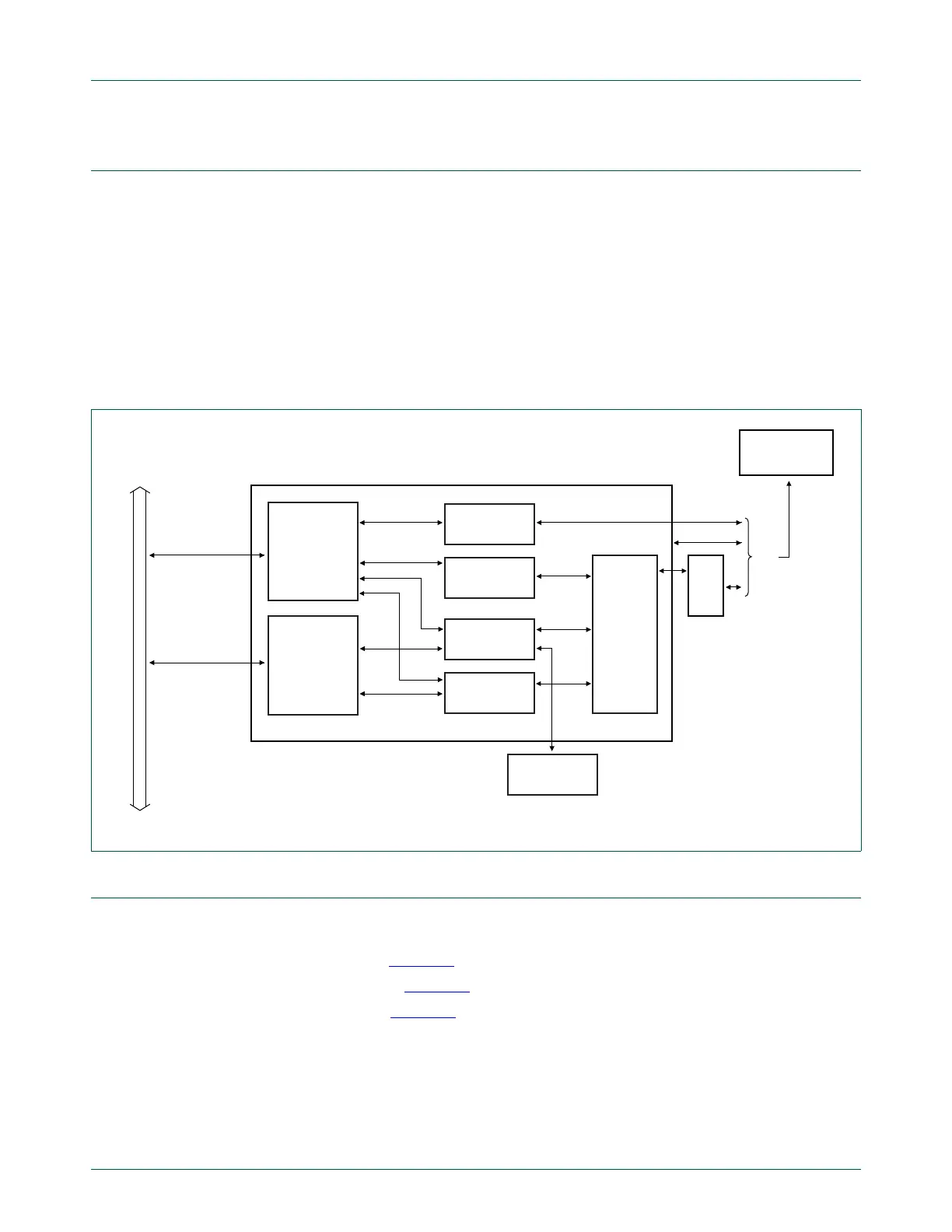
13.5 Architecture
The architecture of the USB OTG controller is shown below in the block diagram.
The host, device, OTG, and I
2
C controllers can be programmed through the register
interface. The OTG controller enables dynamic switching between host and device roles
through the HNP protocol. One port may be connected to an external OTG transceiver to
support an OTG connection. The communication between the register interface and an
external OTG transceiver is handled through an I
2
C interface and through the external
OTG transceiver interrupt signal.
For USB connections that use the device or host controller only (not OTG), the ports use
an embedded USB Analog Transceiver (ATX).
13.6 Modes of operation
The OTG controller is capable of operating in the following modes:
• Host mode (see Figure 35)
• Device mode (see Figure 36)
• OTG mode (see Figure 37)
Fig 34. USB OTG controller block diagram
REGISTER
INTERFACE
BUS
MASTER
INTERFACE
USB
ATX
DMA interface
(AHB master)
register
interface
(AHB slave)
AHB bus
I2C
CONTROLLER
DEVICE
CONTROLLER
HOST
CONTROLLER
EP_RAM
OTG
CONTROLLER
ATX
CONTROL
LOGIC/
PORT
MUX
USB
port
OTG
TRANSCEIVER
USB OTG BLOCK

 Loading...


