UM10360 All information provided in this document is subject to legal disclaimers. © NXP B.V. 2013. All rights reserved.
User manual Rev. 3 — 19 December 2013 109 of 841
NXP Semiconductors
UM10360
Chapter 8: LPC176x/5x Pin connect block
8.5.1 Pin Function Select register 0 (PINSEL0 - 0x4002 C000)
The PINSEL0 register controls the functions of the lower half of Port 0. The direction
control bit in FIO0DIR register is effective only when the GPIO function is selected for a
pin. For other functions, the direction is controlled automatically.
[1] Not available on 80-pin package.
8.5.2 Pin Function Select Register 1 (PINSEL1 - 0x4002 C004)
The PINSEL1 register controls the functions of the upper half of Port 0. The direction
control bit in the FIO0DIR register is effective only when the GPIO function is selected for
a pin. For other functions the direction is controlled automatically.
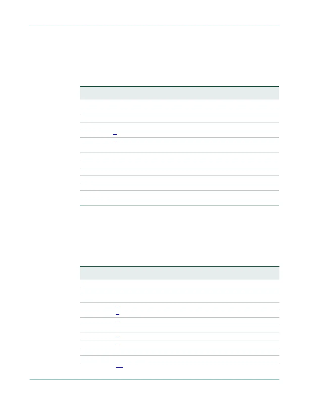
Table 79. Pin function select register 0 (PINSEL0 - address 0x4002 C000) bit description
PINSEL0 Pin
name
Function when
00
Function when 01 Function
when 10
Function
when 11
Reset
value
1:0 P0.0 GPIO Port 0.0 RD1 TXD3 SDA1 00
3:2 P0.1 GPIO Port 0.1 TD1 RXD3 SCL1 00
5:4 P0.2 GPIO Port 0.2 TXD0 AD0.7 Reserved 00
7:6 P0.3 GPIO Port 0.3 RXD0 AD0.6 Reserved 00
9:8 P0.4
[1]
GPIO Port 0.4 I2SRX_CLK RD2 CAP2.0 00
11:10 P0.5
[1]
GPIO Port 0.5 I2SRX_WS TD2 CAP2.1 00
13:12 P0.6 GPIO Port 0.6 I2SRX_SDA SSEL1 MAT2.0 00
15:14 P0.7 GPIO Port 0.7 I2STX_CLK SCK1 MAT2.1 00
17:16 P0.8 GPIO Port 0.8 I2STX_WS MISO1 MAT2.2 00
19:18 P0.9 GPIO Port 0.9 I2STX_SDA MOSI1 MAT2.3 00
21:20 P0.10 GPIO Port 0.10 TXD2 SDA2 MAT3.0 00
23:22 P0.11 GPIO Port 0.11 RXD2 SCL2 MAT3.1 00
29:24 - Reserved Reserved Reserved Reserved 0
31:30 P0.15 GPIO Port 0.15 TXD1 SCK0 SCK 00
Table 80. Pin function select register 1 (PINSEL1 - address 0x4002 C004) bit
description
PINSEL1 Pin name Function when
00
Function
when 01
Function
when 10
Function
when 11
Reset
value
1:0 P0.16 GPIO Port 0.16 RXD1 SSEL0 SSEL 00
3:2 P0.17 GPIO Port 0.17 CTS1 MISO0 MISO 00
5:4 P0.18 GPIO Port 0.18 DCD1 MOSI0 MOSI 00
7:6 P0.19
[1]
GPIO Port 0.19 DSR1 Reserved SDA1 00
9:8 P0.20
[1]
GPIO Port 0.20 DTR1 Reserved SCL1 00
11:10 P0.21
[1]
GPIO Port 0.21 RI1 Reserved RD1 00
13:12 P0.22 GPIO Port 0.22 RTS1 Reserved TD1 00
15:14 P0.23
[1]
GPIO Port 0.23 AD0.0 I2SRX_CLK CAP3.0 00
17:16 P0.24
[1]
GPIO Port 0.24 AD0.1 I2SRX_WS CAP3.1 00
19:18 P0.25 GPIO Port 0.25 AD0.2 I2SRX_SDA TXD3 00
21:20 P0.26 GPIO Port 0.26 AD0.3 AOUT RXD3 00
23:22 P0.27
[1][2]
GPIO Port 0.27 SDA0 USB_SDA Reserved 00

 Loading...


