DocID024597 Rev 3 79/1693
RM0351 Embedded Flash memory (FLASH)
120
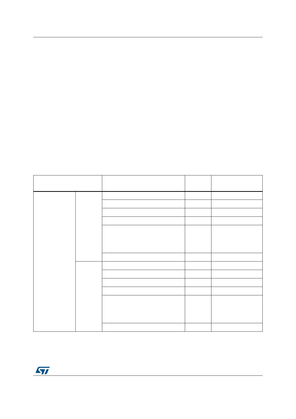
The Flash memory is divided in 2 banks. Each bank is organized as follows:
• A Main memory block containing 256 pages of 2 KBytes. Each page is made of 8 rows
of 256 Bytes.
• An Information block containing:
– System memory from which the device boots in System memory boot mode. The
area is reserved for use by STMicroelectronics and contains the boot loader which
is used to reprogram the Flash memory through one of the following interfaces:
USART1, USART2, USART3, USB (DFU), I2C1, I2C2, I2C3, SPI1, SPI2, SPI3. It
is programmed by STMicroelectronics when the device is manufactured, and
protected against spurious write/erase operations. For further details, please refer
to the AN2606 available from www.st.com.
– 1 KByte (128 double word) OTP (one-time programmable) bytes for user data.
The OTP area is available in Bank 1 only. The OTP data cannot be erased and
can be written only once. If only one bit is at 0, the entire double word cannot be
written anymore, even with the value 0x0000 0000 0000 0000.
– Option bytes for user configuration.
The memory organization is based on a main area and an information block as shown in
Table 5.
Table 5. Flash module - 1 MB dual bank organization
Flash area Flash memory addresses
Size
(bytes)
Name
Main memory
Bank 1
0x0800 0000 - 0x0800 07FF 2 K Page 0
0x0800 0800 - 0x0800 0FFF 2 K Page 1
0x0800 1000 - 0x0800 17FF 2 K Page 2
0x0800 1800 - 0x0800 1FFF 2 K Page 3
-
-
-
-
-
-
-
-
-
-
-
-
0x0807 F800 - 0x0807 FFFF 2 K Page 255
Bank 2
0x0808 0000 - 0x0808 07FF 2 K Page 256
0x0808 0800 - 0x0808 0FFF 2 K Page 257
0x0808 1000 - 0x0808 17FF 2 K Page 258
0x0808 1800 - 0x0808 1FFF 2 K Page 259
-
-
-
-
-
-
-
-
-
-
-
-
0x080F F800 - 0x080F FFFF 2 K Page 511