Flexible static memory controller (FSMC) RM0351
350/1693 DocID024597 Rev 3
14.5.1 External memory interface signals
Table 51, Table 52 and Table 53 list the signals that are typically used to interface with NOR
Flash memory, SRAM and PSRAM.
Note: The prefix “N” identifies the signals which are active low.
NOR Flash memory, non-multiplexed I/Os
The maximum capacity is 512 Mbits (26 address lines).
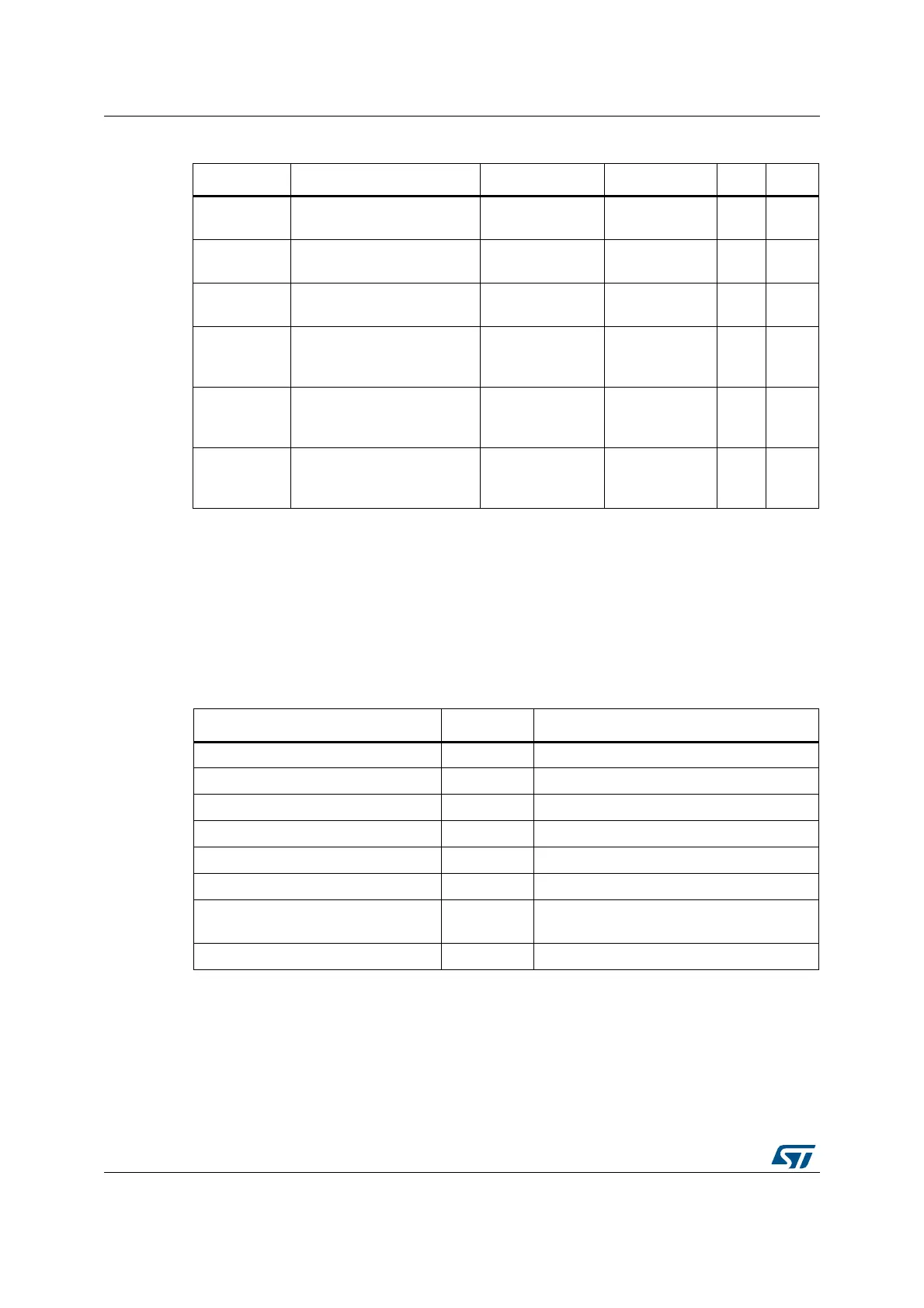
Table 50. Programmable NOR/PSRAM access parameters
Parameter Function Access mode Unit Min. Max.
Address
setup
Duration of the address
setup phase
Asynchronous
AHB clock cycle
(HCLK)
015
Address hold
Duration of the address hold
phase
Asynchronous,
muxed I/Os
AHB clock cycle
(HCLK)
115
Data setup
Duration of the data setup
phase
Asynchronous
AHB clock cycle
(HCLK)
1256
Bust turn
Duration of the bus
turnaround phase
Asynchronous and
synchronous read
/ write
AHB clock cycle
(HCLK)
015
Clock divide
ratio
Number of AHB clock cycles
(HCLK) to build one memory
clock cycle (CLK)
Synchronous
AHB clock cycle
(HCLK)
2 16
Data latency
Number of clock cycles to
issue to the memory before
the first data of the burst
Synchronous
Memory clock
cycle (CLK)
2 17
Table 51. Non-multiplexed I/O NOR Flash memory
FMC signal name I/O Function
CLK O Clock (for synchronous access)
A[25:0] O Address bus
D[15:0] I/O Bidirectional data bus
NE[x] O Chip Select, x = 1..4
NOE O Output enable
NWE O Write enable
NL(=NADV) O
Latch enable (this signal is called address
valid, NADV, by some NOR Flash devices)
NWAIT I NOR Flash wait input signal to the FMC

 Loading...


