DocID024597 Rev 3 115/1693
RM0351 Embedded Flash memory (FLASH)
120
Access: no wait state when no Flash memory operation is on going, word, half-word access
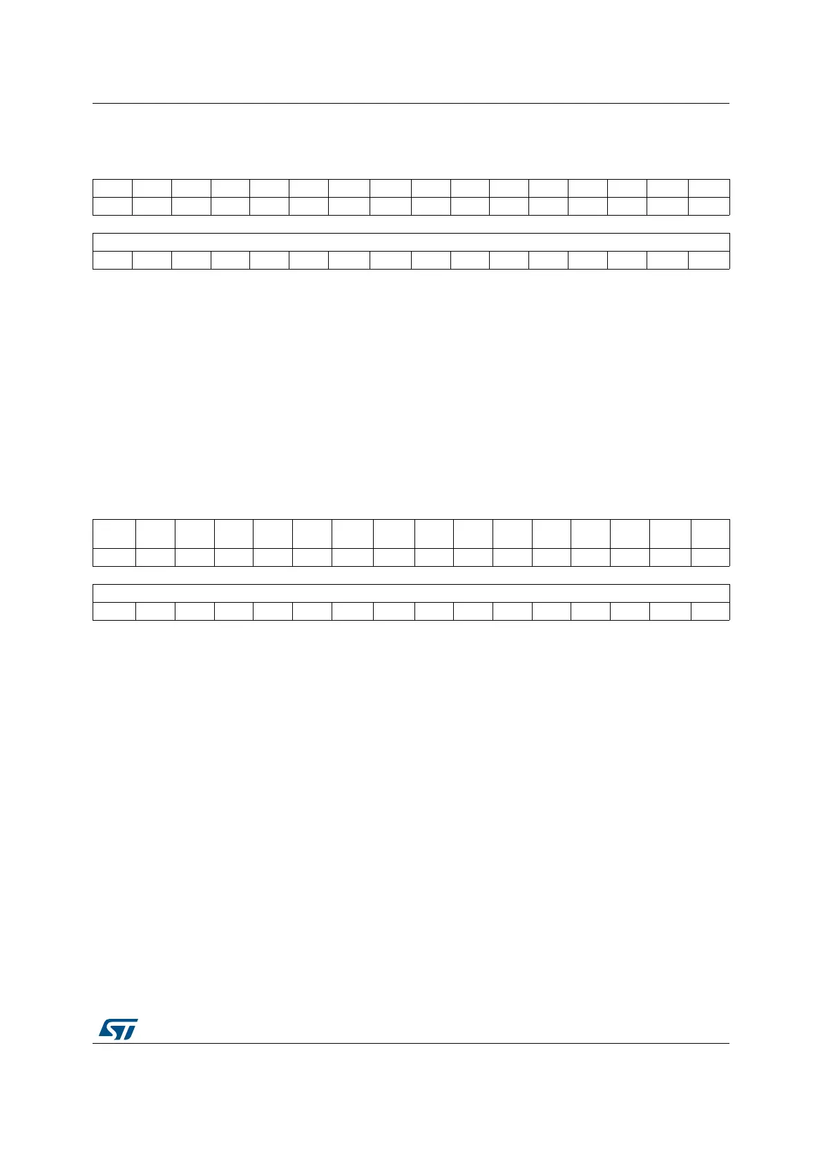
3.7.10 Flash Bank 1 PCROP End address register (FLASH_PCROP1ER)
Address offset: 0x28
Reset value: 0xX000 XXXX
Access: no wait state when no Flash memory operation is on going, word, half-word access.
PCROP_RDP bit can be accessed with byte access
3.7.11 Flash Bank 1 WRP area A address register (FLASH_WRP1AR)
Address offset: 0x2C
Reset value: 0x00XX 00XX
Access: no wait state when no Flash memory operation is on going, word, half-word and
byte access
31 30 29 28 27 26 25 24 23 22 21 20 19 18 17 16
Res. Res. Res. Res. Res. Res. Res. Res. Res. Res. Res. Res. Res. Res. Res. Res.
1514131211109 8765432 1 0
PCROP1_STRT[15:0]
rw rw rw rw rw rw rw rw rw rw rw rw rw rw rw rw
Bits 31:16 Reserved, must be kept cleared
Bits 15:0 PCROP1_STRT: Bank 1 PCROP area start offset
PCROP1_STRT contains the first double-word of the PCROP area.
31 30 29 28 27 26 25 24 23 22 21 20 19 18 17 16
PCROP
_RDP
Res. Res. Res. Res. Res. Res. Res. Res. Res. Res. Res. Res. Res. Res. Res.
rs
15 14 13 12 11 10 9 8 7 6 5 4 3 2 1 0
PCROP1_END[15:0]
rw rw rw rw rw rw rw rw rw rw rw rw rw rw rw rw
Bit 31 PCROP_RDP: PCROP area preserved when RDP level decreased
This bit is set only. It is reset after a full mass erase due to a change of RDP
from Level 1 to Level 0.
0: PCROP area is not erased when the RDP level is decreased from Level 1 to
Level 0.
1: PCROP area is erased when the RDP level is decreased from Level 1 to
Level 0 (full mass erase).
Bits 30:16 Reserved, must be kept cleared
Bits 15:0 PCROP1_END: Bank 1 PCROP area end offset
PCROP1_END contains the last double-word of the bank 1 PCROP area.