Embedded Flash memory (FLASH) RM0351
118/1693 DocID024597 Rev 3
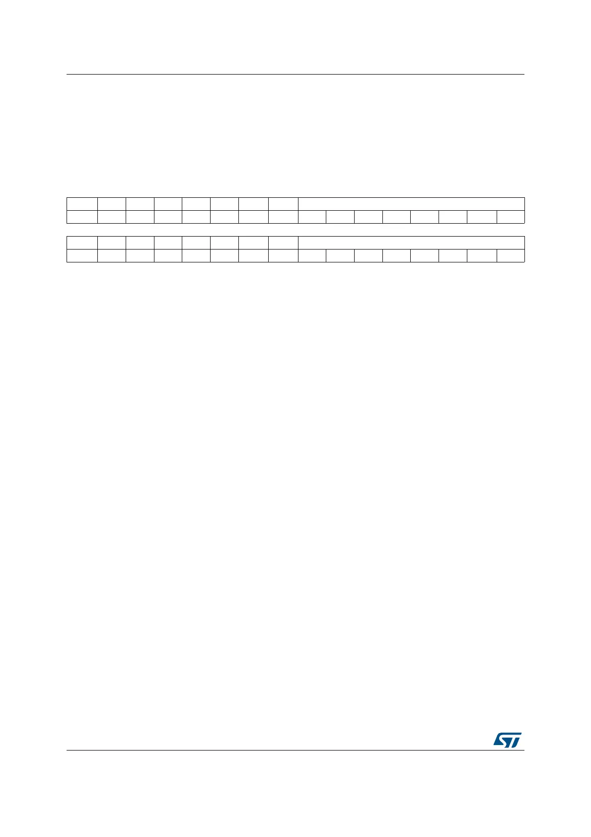
3.7.16 Flash Bank 2 WRP area B address register (FLASH_WRP2BR)
Address offset: 0x50
Reset value: 0x00XX 00XX
Access: no wait state when no Flash memory operation is on going, word, half-word and
byte access
31 30 29 28 27 26 25 24 23 22 21 20 19 18 17 16
Res. Res. Res. Res. Res. Res. Res. Res. WRP2B_END[7:0]
rw rw rw rw rw rw rw rw
15 14 13 12 11 10 9 8 7 6 5 4 3 2 1 0
Res. Res. Res. Res. Res. Res. Res. Res. WRP2B_STRT[7:0]
rw rw rw rw rw rw rw rw
Bits 31:24 Reserved, must be kept cleared
Bits 23:16 WRP2B_END: Bank 2 WRP second area “B” end offset
WRP2B_END contains the last page of the bank 2 WRP second area.
Bits 15:8 Reserved, must be kept cleared
Bits 7:0 WRP2B_STRT: Bank 2 WRP second area “B” start offset
WRP2B_STRT contains the first page of the bank 2 WRP second area.

 Loading...


