DocID024597 Rev 3 67/1693
RM0351
77
All the memory areas that are not allocated to on-chip memories and peripherals are
considered “Reserved”. For the detailed mapping of available memory and register areas,
please refer to Memory map and register boundary addresses and peripheral sections.
2.2.2 Memory map and register boundary addresses
See the datasheet corresponding to your device for a comprehensive diagram of the
memory map.
The following table gives the boundary addresses of the peripherals available in the
devices.
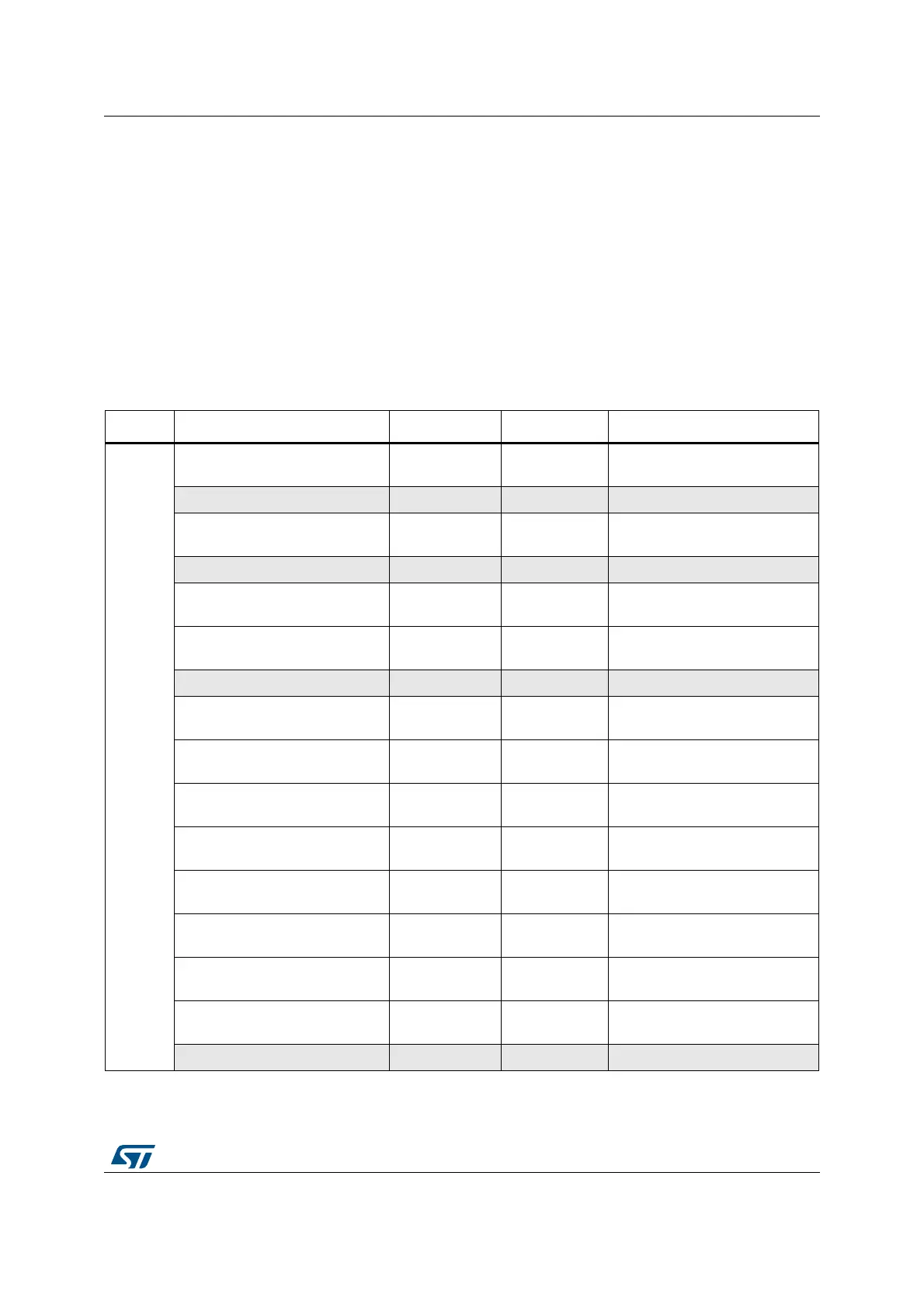
Table 1. STM32L4x6 memory map and peripheral register boundary addresses
Bus Boundary address Size (bytes) Peripheral Peripheral register map
AHB2
0x5006 0800 - 0x5006 0BFF 1 KB RNG
Section 24.4.4: RNG register
map
0x5006 0400 - 0x5006 07FF 1KB Reserved -
0x5006 0000 - 0x5006 03FF 1 KB AES
Section 25.14.18: AES register
map
0x5004 0400 - 0x5005 FFFF 127 KB Reserved -
0x5004 0000 - 0x5004 03FF 1 KB ADC
Section 16.6.4: ADC register
map
0x5000 0000 - 0x5003 FFFF 16 KB OTG_FS
Section 43.15.54: OTG_FS
register map
0x4800 2000 - 0x4FFF FFFF ~127 MB Reserved -
0x4800 1C00 - 0x4800 1FFF 1 KB GPIOH
Section 7.4.13: GPIO register
map
0x4800 1800 - 0x4800 1BFF 1 KB GPIOG
Section 7.4.13: GPIO register
map
0x4800 1400 - 0x4800 17FF 1 KB GPIOF
Section 7.4.13: GPIO register
map
0x4800 1000 - 0x4800 13FF 1 KB GPIOE
Section 7.4.13: GPIO register
map
0x4800 0C00 - 0x4800 0FFF 1 KB GPIOD
Section 7.4.13: GPIO register
map
0x4800 0800 - 0x4800 0BFF 1 KB GPIOC
Section 7.4.13: GPIO register
map
0x4800 0400 - 0x4800 07FF 1 KB GPIOB
Section 7.4.13: GPIO register
map
0x4800 0000 - 0x4800 03FF 1 KB GPIOA
Section 7.4.13: GPIO register
map
0x4002 4400 - 0x47FF FFFF ~127 MB Reserved -