Digital-to-analog converter (DAC) RM0351
550/1693 DocID024597 Rev 3
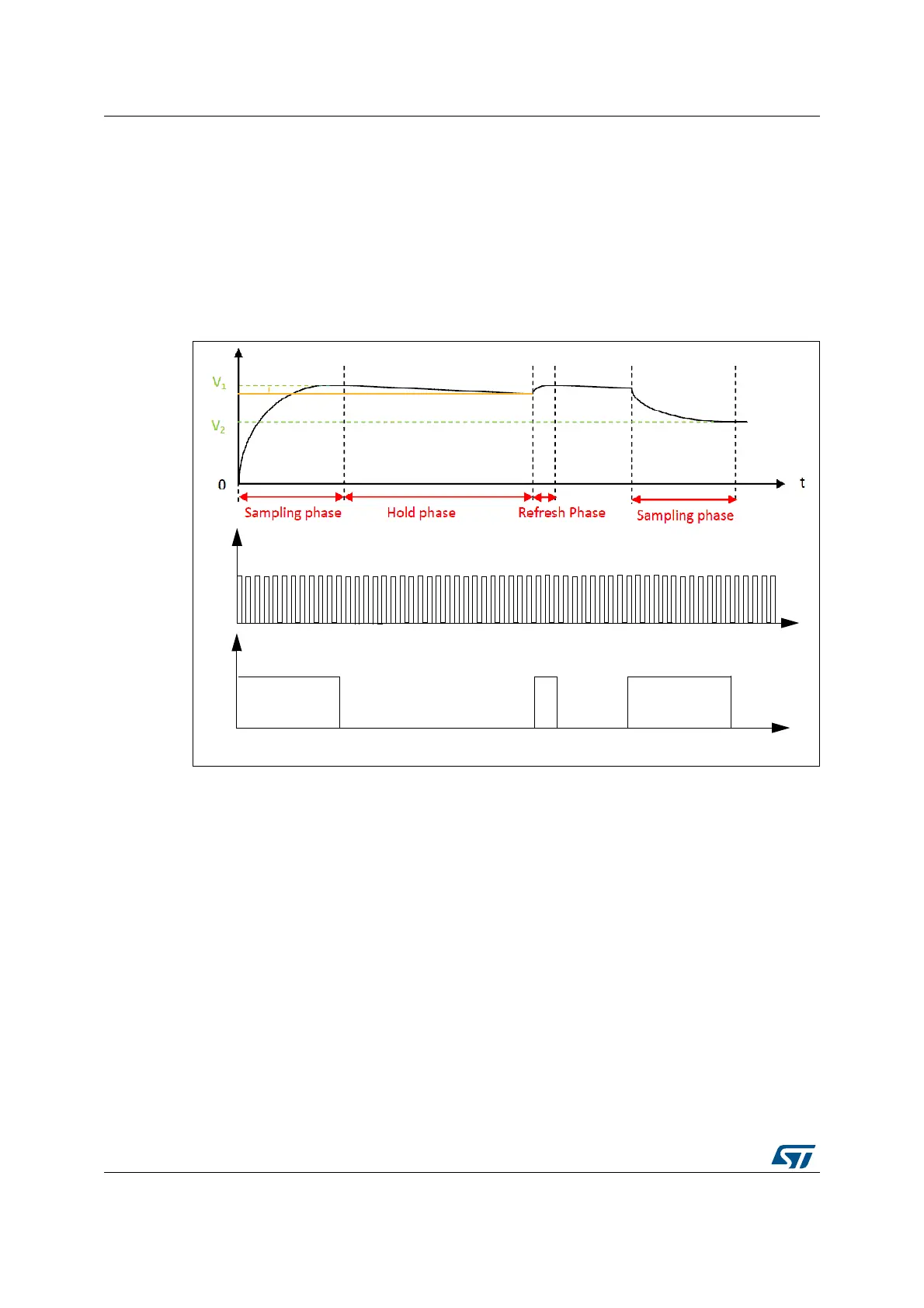
Refresh phase:
t
refresh
= 7 s + (2000 * 100 * 10
-9
) * ln(2*10) = 606.1 s
(where N
lsb
= 10 (10 LSB drop during the hold phase)
Hold phase:
D
v
= i
leak
* t
hold
/ C
load
= 0.0073 V (10 LSB of 12bit at 3 V)
i
leak
= 150 nA (worst case on the IO leakage on all the temperature range)
t
hold
= 0.0073 * 100 * 10
-9
/ (150 * 10
-9
) = 4.867 ms
Figure 137. DAC sample and hold mode phases diagram
Like in normal mode, the sample and hold mode has different configurations.
To enable the output buffer, the MODEx[2:0] bits in DAC_MCR register should be:
– 100: DAC is connected to the external pin
– 101: DAC is connected to external pin and to on chip peripherals
To disabled the output buffer, The MODEx[2:0] bits in DAC_MCR register should be:
– 110: DAC is connected to external pin and to on chip peripherals
– 111: DAC is connected to on chip peripherals
When MODEx[2:0] bits in DAC_MCR register is equal to 111. An internal capacitor “C
loadint“
will hold the voltage output of the DAC Core and then drive it to on-chip peripherals.
All sample and hold phases are interruptible and any change in DAC_DHRx will trigger
immediately a new sample phase.