Power control (PWR) RM0351
162/1693 DocID024597 Rev 3
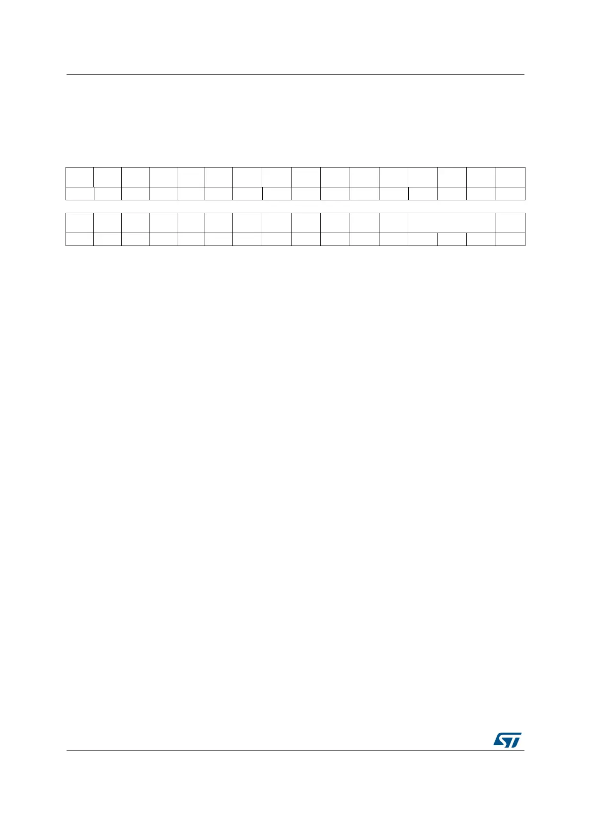
5.4.2 Power control register 2 (PWR_CR2)
Address offset: 0x04
Reset value: 0x0000 0000. This register is reset when exiting the Standby mode.
31 30 29 28 27 26 25 24 23 22 21 20 19 18 17 16
Res. Res. Res. Res. Res. Res. Res. Res. Res. Res. Res. Res. Res. Res. Res. Res.
1514131211109876543210
Res. Res. Res. Res. Res. USV IOSV Res. PVME4 PVME3 PVME2 PVME1 PLS[2:0] PVDE
rw rw rw rw rw rw rw rw rw rw
Bits 31:11 Reserved, must be kept at reset value.
Bit 10 USV:
V
DDUSB
USB supply valid
This bit is used to validate the
V
DDUSB
supply for electrical and logical isolation purpose.
Setting this bit is mandatory to use the USB OTG_FS peripheral. If
V
DDUSB
is not always
present in the application, the PVM can be used to determine whether this supply is ready or
not.
0:
V
DDUSB
is not present. Logical and electrical isolation is applied to ignore this supply.
1:
V
DDUSB
is valid.
Bit 9 IOSV:
V
DDIO2
Independent I/Os supply valid
This bit is used to validate the
V
DDIO2
supply for electrical and logical isolation purpose.
Setting this bit is mandatory to use PG[15:2]. If
V
DDIO2
is not always present in the
application, the PVM can be used to determine whether this supply is ready or not.
0:
V
DDIO2
is not present. Logical and electrical isolation is applied to ignore this supply.
1:
V
DDIO2
is valid.
Bit 8 Reserved, must be kept at reset value.
Bit 7 PVME4: Peripheral voltage monitoring 4 enable: V
DDA
vs. 2.2V
0: PVM4 (V
DDA
monitoring vs. 2.2V threshold) disable.
1: PVM4 (
V
DDA
monitoring vs. 2.2V threshold) enable.
Bit 6 PVME3: Peripheral voltage monitoring 3 enable:
V
DDA
vs. 1.62V
0: PVM3 (V
DDA
monitoring vs. 1.62V threshold) disable.
1: PVM3 (
V
DDA
monitoring vs. 1.62V threshold) enable.
Bit 5 PVME2: Peripheral voltage monitoring 2 enable:
V
DDIO2
vs. 0.9V
0: PVM2 (V
DDIO2
monitoring vs. 0.9V threshold) disable.
1: PVM2 (
V
DDIO2
monitoring vs. 0.9V threshold) enable.