Analog-to-digital converters (ADC) RM0351
534/1693 DocID024597 Rev 3
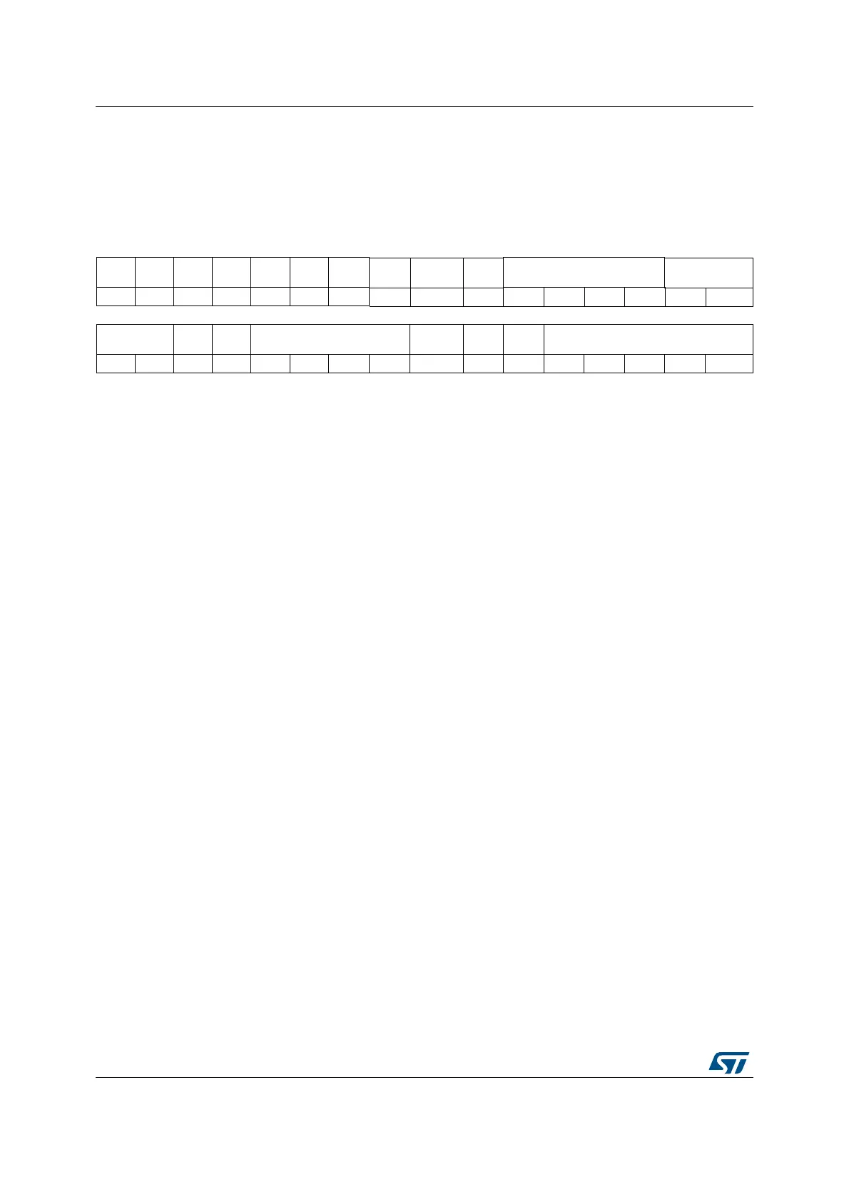
16.6.2 ADC common control register (ADCx_CCR)
Address offset: 0x08 (this offset address is relative to the master ADC base address +
0x300)
Reset value: 0x0000 0000
31 30 29 28 27 26 25 24 23 22 21 20 19 18 17 16
Res. Res. Res. Res. Res. Res. Res.
CH18
SEL
CH17
SEL
VREF
EN
PRESC[3:0] CKMODE[1:0]
rw rw rw rw rw rw rw rw rw
15141312111098 7 654321 0
MDMA[1:0]
DMA
CFG
Res. DELAY[3:0] Res. Res. Res. DUAL[4:0]
rw rw rw rw rw rw rw rw rw rw rw rw
Bits 31:25 Reserved, must be kept at reset value.
Bit 24 CH18SEL: CH18 selection
This bit is set and cleared by software to control the channel 18 of ADC1 and ADC3
0: V
BAT
channel disabled.
1: V
BAT
channel enabled
Note: Software is allowed to write this bit only when the ADCs are disabled (ADCAL=0,
JADSTART=0, ADSTART=0, ADSTP=0, ADDIS=0 and ADEN=0).
Bit 23 CH17SEL: CH17 selection
This bit is set and cleared by software to control the channel 17 of ADC1 and ADC3
0: Temperature sensor channel disabled
1: Temperature sensor channel enabled
Note: Software is allowed to write this bit only when the ADCs are disabled (ADCAL=0,
JADSTART=0, ADSTART=0, ADSTP=0, ADDIS=0 and ADEN=0).
Bit 22 VREFEN: V
REFINT
enable
This bit is set and cleared by software to enable/disable the V
REFINT
channel.
0: V
REFINT
channel disabled
1: V
REFINT
channel enabled
Note: Software is allowed to write this bit only when the ADCs are disabled (ADCAL=0,
JADSTART=0, ADSTART=0, ADSTP=0, ADDIS=0 and ADEN=0).