DocID024597 Rev 3 629/1693
RM0351 Digital filter for sigma delta modulators (DFSDM)
657
21.5 DFSDM DMA transfer
To decrease the CPU intervention, conversions can be transferred into memory using a
DMA transfer. A DMA transfer for injected conversions is enabled by setting bit JDMAEN=1
in DFSDMx_CR1 register. A DMA transfer for regular conversions is enabled by setting bit
RDMAEN=1 in DFSDMx_CR1 register.
Note: With a DMA transfer, the interrupt flag is automatically cleared at the end of the injected or
regular conversion (JEOCF or REOCF bit in DFSDMx_ISR register) because DMA is
reading DFSDMx_JDATAR or DFSDMx_RDATAR register.
21.6 DFSDM channel y registers (y=0..7)
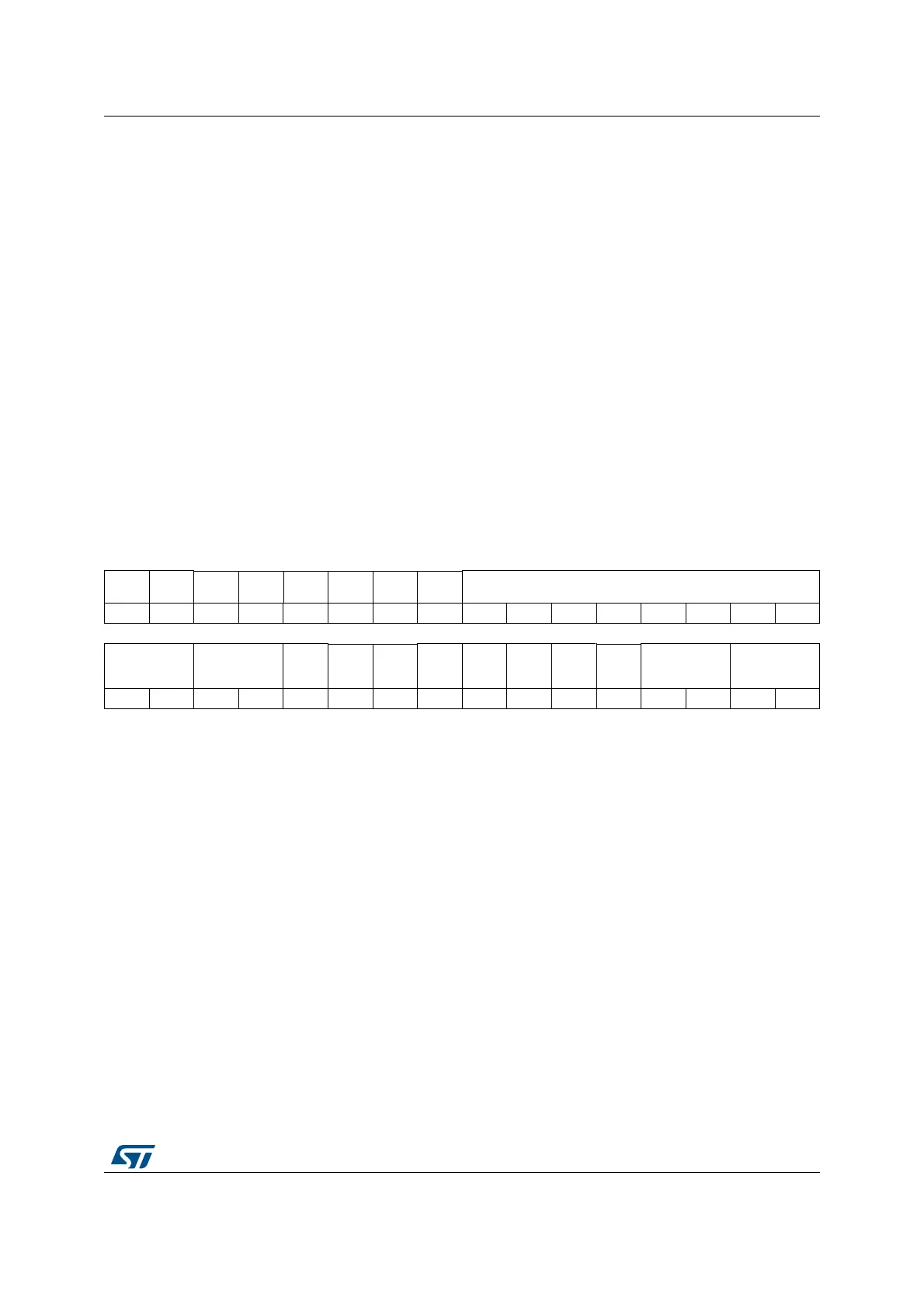
21.6.1 DFSDM channel configuration y register (DFSDM_CHCFGyR1)
(y=0..7)
This register specifies the parameters used by channel y (y = 0..7).
Address offset: 0x00
Reset value: 0x0000 0000
31 30 29 28 27 26 25 24 23 22 21 20 19 18 17 16
DFSDM
EN
CKOUT
SRC
Res. Res. Res. Res. Res. Res. CKOUTDIV[7:0]
rw rw rw rw rw rw rw rw rw rw
1514131211109876543210
DATPACK[1:0] DATMPX[1:0] Res. Res. Res.
CHIN
SEL
CHEN
CKAB
EN
SCDEN Res. SPICKSEL[1:0] SITP[1:0]
rw rw rw rw rw rw rw rw rw rw rw rw
Bit 31 DFSDMEN: Global enable for DFSDM interface
0: DFSDM interface disabled
1: DFSDM interface enabled
If DFSDM interface is enabled, then it is started to operate according to enabled y channels and
enabled x filters settings (CHEN bit in DFSDM_CHCFGyR1 and DFEN bit in DFSDMx_CR1). Data
cleared by setting DFSDMEN=0:
–all registers DFSDMx_ISR ars set to reset state (x = 0..3)
–all registers DFSDMx_AWSR are set to reset state (x = 0..3)
Note: DFSDMEN is present only in DFSDM_CHCFG0R1 register (channel y=0)
Bit 30 CKOUTSRC: Output serial clock source selection
0: Source for output clock is from system clock
1: Source for output clock is from audio clock
–SAI1 clock selected by SAI1SEL[1:0] field in RCC configuration (see Section 6.4.28: Peripherals
independent clock configuration register (RCC_CCIPR))
This value can be modified only when DFSDMEN=0 (in DFSDM_CHCFG0R1 register).
Note: CKOUTSRC is present only in DFSDM_CHCFG0R1 register (channel y=0)
Bits 29:24 Reserved, must be kept at reset value.

 Loading...


