Liquid crystal display controller (LCD) RM0351
682/1693 DocID024597 Rev 3
Note: The VSEL, MUX_SEG, BIAS, DUTY and BUFEN bits are write-protected when the LCD is
enabled (ENS bit in LCD_SR to 1).
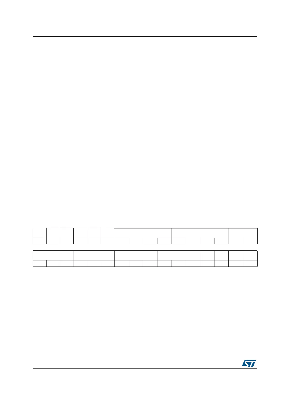
22.6.2 LCD frame control register (LCD_FCR)
Address offset: 0x04
Reset value: 0x0000 0000
Bits 4:2 DUTY[2:0]: Duty selection
These bits determine the duty cycle. Values 101, 110 and 111 are forbidden.
000: Static duty
001: 1/2 duty
010: 1/3 duty
011: 1/4 duty
100: 1/8 duty
101: Reserved
110: Reserved
111: Reserved
Bit 1 VSEL: Voltage source selection
The VSEL bit determines the voltage source for the LCD.
0: Internal source (voltage step-up converter)
1: External source (VLCD pin)
Bit 0 LCDEN: LCD controller enable
This bit is set by software to enable the LCD Controller/Driver. It is cleared by software to turn
off the LCD at the beginning of the next frame. When the LCD is disabled all COM and SEG
pins are driven to V
SS
.
0: LCD Controller disabled
1: LCD Controller enabled
31 30 29 28 27 26 25 24 23 22 21 20 19 18 17 16
Res. Res. Res. Res. Res. Res. PS[3:0] DIV[3:0] BLINK[1:0]
rw rw rw rw rw rw rw rw rw rw
15 14 13 12 11 10 9 8 7 6 5 4 3 2 1 0
BLINKF[2:0] CC[2:0] DEAD[2:0] PON[2:0] UDDIE Res. SOFIE HD
rw rw rw rw rw rw rw rw rw rw rw rw rw rw rw