DocID024597 Rev 3 1653/1693
RM0351 Debug support (DBG)
1678
44.6.4 Cortex
®
-M4 JEDEC-106 ID code
The ARM
®
Cortex
®
-M4 integrates a JEDEC-106 ID code. It is located in the 4KB ROM table
mapped on the internal PPB bus at address 0xE00FF000_0xE00FFFFF.
This code is accessible by the JTAG Debug Port (4 to 5 pins) or by the SW Debug Port (two
pins) or by the user software.
44.7 JTAG debug port
A standard JTAG state machine is implemented with a 4-bit instruction register (IR) and five
data registers (for full details, refer to the Cortex
®
-M4 with FPU r0p1 Technical Reference
Manual (TRM), for references, please see Section 44.2: Reference ARM® documentation).
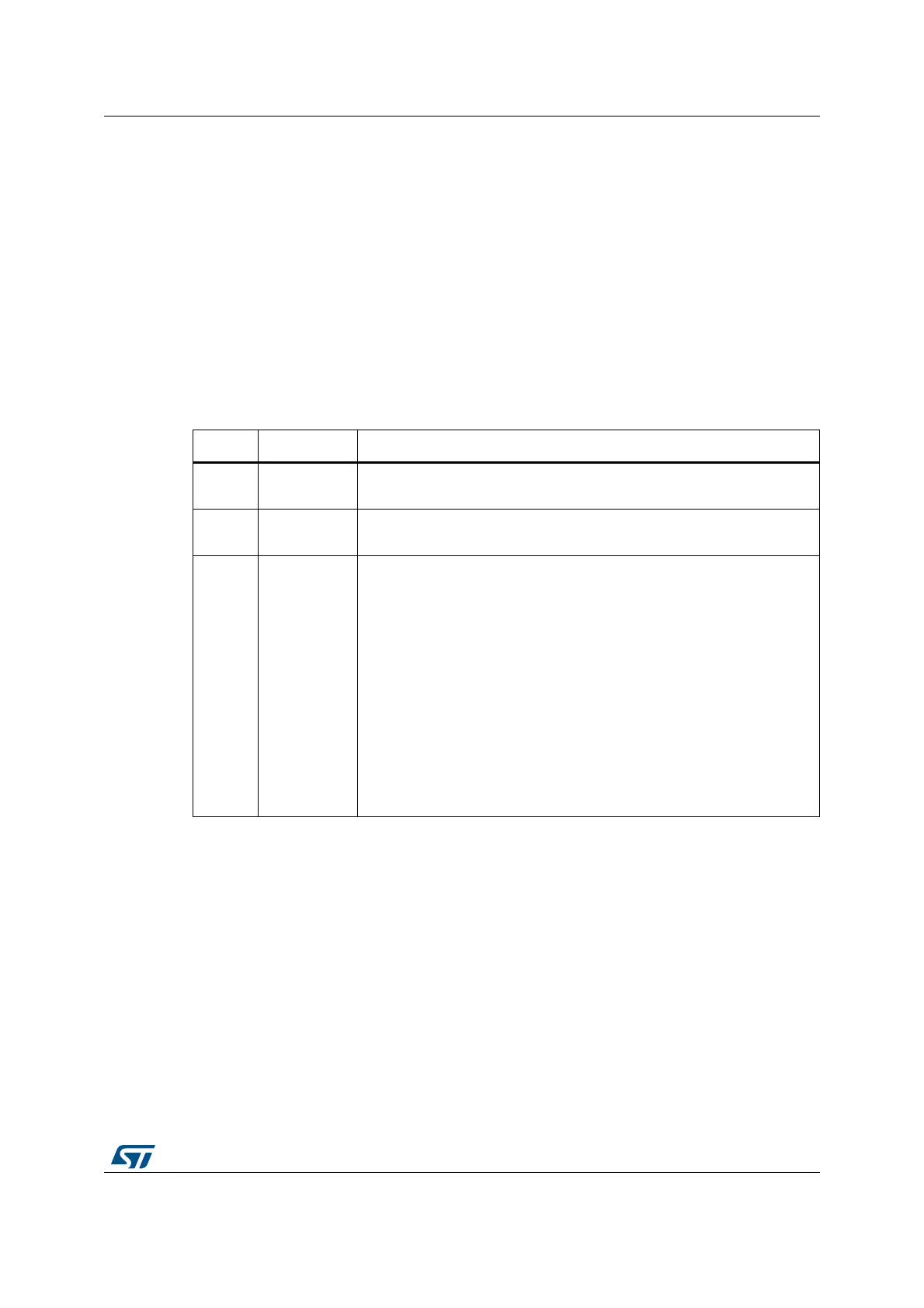
Table 266. JTAG debug port data registers
IR(3:0) Data register Details
1111
BYPASS
[1 bit]
-
1110
IDCODE
[32 bits]
ID CODE
0x3BA00477 (ARM
®
Cortex
®
-M4 r0p1-01rel0 ID Code)
1010
DPACC
[35 bits]
Debug port access register
This initiates a debug port and allows access to a debug port register.
– When transferring data IN:
Bits 34:3= DATA[31:0] = 32-bit data to transfer for a write request
Bits 2:1 = A[3:2] = 2-bit address of a debug port register.
Bit 0 = RnW = Read request (1) or write request (0).
– When transferring data OUT:
Bits 34:3 = DATA[31:0] = 32-bit data which is read following a read
request
Bits 2:0 = ACK[2:0] = 3-bit Acknowledge:
010 = OK/FAULT
001 = WAIT
OTHER = reserved
Refer to Table 267 for a description of the A(3:2) bits

 Loading...


