DocID024597 Rev 3 75/1693
RM0351
77
CPU code execution. It also implements the logic necessary to carry out the Flash memory
operations (Program/Erase) controlled through the Flash registers. Refer to Section 3:
Embedded Flash memory (FLASH) for more details.
2.6 Boot configuration
In the STM32L4x6, three different boot modes can be selected through the BOOT0 pin and
nBOOT1 bit in the User option byte, as shown in the following table.
The values on both BOOT0 pin and nBOOT1 bit are latched after a reset. It is up to the user
to set nBOOT1 and BOOT0 to select the required boot mode.
The BOOT0 pin and nBOOT1 bit are also re-sampled when exiting from Standby mode.
Consequently they must be kept in the required Boot mode configuration in Standby mode.
After this startup delay has elapsed, the CPU fetches the top-of-stack value from address
0x0000 0000, then starts code execution from the boot memory at 0x0000 0004.
Depending on the selected boot mode, main Flash memory, system memory or SRAM1 is
accessible as follows:
• Boot from main Flash memory: the main Flash memory is aliased in the boot memory
space (0x0000 0000), but still accessible from its original memory space
(0x0800 0000). In other words, the Flash memory contents can be accessed starting
from address 0x0000 0000 or 0x0800 0000.
• Boot from system memory: the system memory is aliased in the boot memory space
(0x0000 0000), but still accessible from its original memory space (0x1FFF 0000).
• Boot from the embedded SRAM1: the SRAM1 is aliased in the boot memory space
(0x0000 0000), but it is still accessible from its original memory space (0x2000 0000).
Note: When the device boots from SRAM, in the application initialization code, you have to
relocate the vector table in SRAM using the NVIC exception table and the offset register.
When booting from the main Flash memory, the application software can either boot from
bank 1 or from bank 2. By default, boot from bank 1 is selected.
To select boot from Flash memory bank 2, set the BFB2 bit in the user option bytes. When
this bit is set and the boot pins are in the boot from main Flash memory configuration, the
device boots from system memory, and the boot loader jumps to execute the user
application programmed in Flash memory bank 2. For further details, please refer to
AN2606.
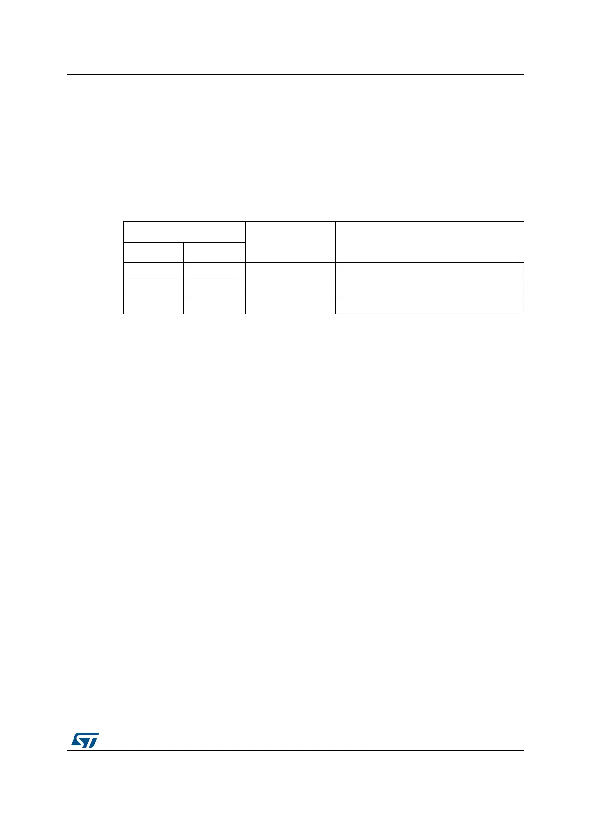
Table 3. Boot modes
Boot mode selection
Boot mode Aliasing
BOOT1
(1)
1. The BOOT1 value is the opposite of the nBOOT1 Option Bit.
BOOT0
x 0 Main Flash memory Main Flash memory is selected as boot area
0 1 System memory System memory is selected as boot area
1 1 Embedded SRAM1 Embedded SRAM1 is selected as boot area