General-purpose timers (TIM15/16/17) RM0351
978/1693 DocID024597 Rev 3
Note: The state of the external I/O pins connected to the complementary OCx and OCxN channels
depends on the OCx and OCxN channel state and AFIO registers.
Bit 0 CC1E: Capture/Compare 1 output enable
CC1 channel configured as output:
0: Off - OC1 is not active. OC1 level is then function of MOE, OSSI, OSSR, OIS1, OIS1N
and CC1NE bits.
1: On - OC1 signal is output on the corresponding output pin depending on MOE, OSSI,
OSSR, OIS1, OIS1N and CC1NE bits.
CC1 channel configured as input: This bit determines if a capture of the counter value can
actually be done into the input capture/compare register 1 (TIMx_CCR1) or not.
0: Capture disabled
1: Capture enabled
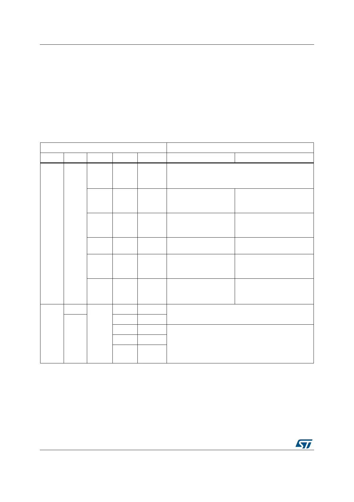
Table 157. Output control bits for complementary OCx and OCxN channels with break feature
Control bits Output states
(1)
MOE bit OSSI bit OSSR bit CCxE bit CCxNE bit OCx output state OCxN output state
1X
X0 0
Output Disabled (not driven by the timer: Hi-Z)
OCx=0
OCxN=0, OCxN_EN=0
00 1
Output Disabled (not driven
by the timer: Hi-Z)
OCx=0
OCxREF + Polarity
OCxN=OCxREF XOR CCxNP
01 0
OCxREF + Polarity
OCx=OCxREF XOR CCxP
Output Disabled (not driven by
the timer: Hi-Z)
OCxN=0
X1 1
OCREF + Polarity + dead-
time
Complementary to OCREF (not
OCREF) + Polarity + dead-time
10 1
Off-State (output enabled
with inactive state)
OCx=CCxP
OCxREF + Polarity
OCxN=OCxREF XOR CCxNP
11 0
OCxREF + Polarity
OCx=OCxREF xor CCxP,
OCx_EN=1
Off-State (output enabled with
inactive state)
OCxN=CCxNP, OCxN_EN=1
0
0
X
XX
Output Disabled (not driven by the timer: Hi-Z)
OCx=CCxP, OCxN=CCxNP
1
00
0 1 Off-State (output enabled with inactive state)
Asynchronously: OCx=CCxP, OCxN=CCxNP
Then if the clock is present: OCx=OISx and OCxN=OISxN
after a dead-time, assuming that OISx and OISxN do not
correspond to OCX and OCxN both in active state
10
11
1. When both outputs of a channel are not used (control taken over by GPIO controller), the OISx, OISxN, CCxP and CCxNP
bits must be kept cleared.