DocID024597 Rev 3 549/1693
RM0351 Digital-to-analog converter (DAC)
573
The sample/hold mode operations can be divided into 3 phases:
1. Sample phase: the sample/hold element is charged to the desired voltage. The
charging time depends on capacitor value (internal or external, selected by the user).
The sampling time is configured with the TSAMx[9:0] bits in DAC_SHSRx register.
During the write of the TSAMx[9:0] bits; the BWSTx bit in DAC_SR register is set to 1 to
synchronize between both clocks domains (APB and low speed clock) and allowing the
software to change the value of sample phase during the DAC channel operation
2. Hold phase: the DAC output channel is tri-stated, the DAC core and the buffer are
turned off, to reduce the current consumption. The hold time is configured with the
THOLDx[9:0] bits in DAC_SHHR register
3. Refresh phase: the refresh time is configured with the TREFx[7:0] bits in DAC_SHRR
register
The timings for the three phases above are in units of LSI clocks. As example, to configure
a Sample time of 350µs, Hold time of 2ms and Refresh time of 100µs assuming LSI ~32KHz
is selected:
12 cycles are required for sample phase: SAMx[9:0] = 11, 62 cycles are required for hold
phase: THOLDx[9:0] = 62, and 4 cycles are required for refresh period: TREFx[7:0] = 4.
In this example, the power consumption is reduced by almost a factor of 15 versus Normal
modes.
The Formulas to compute the right sample and refresh timings are described in the table
below, the Hold time depends on the leakage current.
Note: 1 In the above formula the settling to the desired code value with ½ LSB or accuracy requires
10 constant time for 12 bits resolution. For 8 bits resolution, the settling time is 7 constant
time.
2 The tolerated voltage drop during the hold phase “Vd” is represented by the number of LSBs
after the capacitor discharging with the output leakage current. The settling back to the
desired value with ½ LSB error accuracy requires ln(2*Nlsb) constant time of the DAC.
3 The parameters “T
stab-BON
“,“T
stab-BON
“, “R
BON
” and “R
BOFF
” are specified in the datasheet
Example of the sample and refresh time calculation with output buffer on
Note: The values used in the example below are provided as indication only. Please refer to the
product datasheet for product data.
C
load
= 100 nF
V
DDA
= 3.0 V
Sampling phase:
t
sampling
= 7 s + (10 * 2000 * 100 * 10
-9
) = 2.007 ms
(where T
stab-BON
= 7 s, RBON = 2 k)
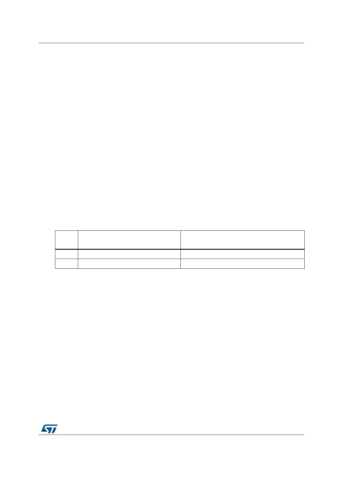
Table 103. Sample and refresh timings
Buffer
State
tsampling (1)(3) trefresh (2)(3)
Enable T
stab-BON
+ (10*R
BON
*C
load
)T
stab-BON
+ (R
BON
*C
load
)*ln(2*Nlsb)
Disable T
stab-BOFF
+ ( 10*R
BOFF
*Cload)T
stab-BOFF
+ (R
BOFF
*Cload)*ln(2*Nlsb)