Embedded Flash memory (FLASH) RM0351
82/1693 DocID024597 Rev 3
When ECCC or ECCD is set, ADDR_ECC and BK_ECC are not updated if a new ECC error
occurs. FLASH_ECCR is updated only when ECC flags are cleared.
Note: For a virgin data: 0xFF FFFF FFFF FFFF FFFF, one error is detected and corrected but 2
errors detection is not supported.
When an ECC error is reported, a new read at the failing address may not generate an ECC
error if the data is still present in the current buffer, even if ECCC and ECCD are cleared.
3.3.3 Read access latency
To correctly read data from Flash memory, the number of wait states (LATENCY) must be
correctly programmed in the Flash access control register (FLASH_ACR) according to the
frequency of the CPU clock (HCLK) and the internal voltage range of the device V
CORE
.
Refer to Section 5.1.7: Dynamic voltage scaling management. Table 8 shows the
correspondence between wait states and CPU clock frequency.
After reset, the CPU clock frequency is 4 MHz and 0 wait state (WS) is configured in the
FLASH_ACR register.
When changing the CPU frequency, the following software sequences must be applied in
order to tune the number of wait states needed to access the Flash memory:
Increasing the CPU frequency:
1. Program the new number of wait states to the LATENCY bits in the Flash access
control register (FLASH_ACR).
2. Check that the new number of wait states is taken into account to access the Flash
memory by reading the FLASH_ACR register
3. Modify the CPU clock source by writing the SW bits in the RCC_CFGR register
4. If needed, modify the CPU clock prescaler by writing the HPRE bits in RCC_CFGR
5. Check that the new CPU clock source or/and the new CPU clock prescaler value is/are
taken into account by reading the clock source status (SWS bits) or/and the AHB
prescaler value (HPRE bits), respectively, in the RCC_CFGR register.
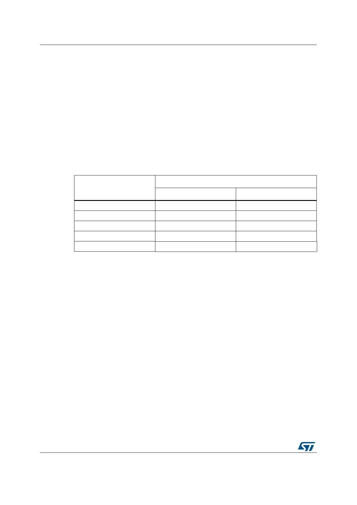
Table 8. Number of wait states according to CPU clock (HCLK) frequency
Wait states (WS)
(LATENCY)
HCLK (MHz)
V
CORE
Range 1 V
CORE
Range 2
0 WS (1 CPU cycles) 16 6
1 WS (2 CPU cycles) 32 12
2 WS (3 CPU cycles) 48 18
3 WS (4 CPU cycles) 64 26
4 WS (5 CPU cycles) 80 26

 Loading...


