DocID024597 Rev 3 841/1693
RM0351 Advanced-control timers (TIM1/TIM8)
856
26.4.20 TIM1/TIM8 DMA address for full transfer (TIMx_DMAR)
Address offset: 0x4C
Reset value: 0x0000
26.4.21 TIM1 option register 1 (TIM1_OR1)
Address offset: 0x50
Reset value: 0x0000 0000
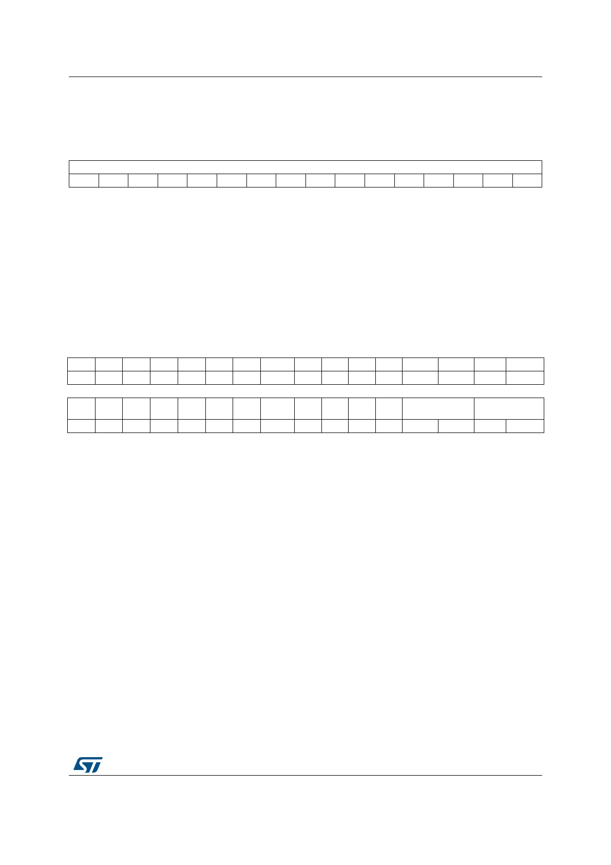
1514131211109876543210
DMAB[15:0]
rw rw rw rw rw rw rw rw rw rw rw rw rw rw rw rw
Bits 15:0 DMAB[15:0]: DMA register for burst accesses
A read or write operation to the DMAR register accesses the register located at the address
(TIMx_CR1 address) + (DBA + DMA index) x 4
where TIMx_CR1 address is the address of the control register 1, DBA is the DMA base
address configured in TIMx_DCR register, DMA index is automatically controlled by the DMA
transfer, and ranges from 0 to DBL (DBL configured in TIMx_DCR).
31 30 29 28 27 26 25 24 23 22 21 20 19 18 17 16
Res. Res. Res. Res. Res. Res. Res. Res. Res. Res. Res. Res. Res. Res. Res. Res.
1514131211109 8 7654 3 2 1 0
Res. Res. Res. Res. Res. Res. Res. Res. Res. Res. Res.
TI1_R
MP
ETR_ADC3_RMP ETR_ADC1_RMP
rw rw rw rw rw
Bits 31:5 Reserved, must be kept at reset value
Bit 4 TI1_RMP: Input Capture 1 remap
0: TIM1 input capture 1 is connected to I/O
1: TIM1 input capture 1 is connected to COMP1 output.
Bits 3:2 ETR_ADC3_RMP: External trigger remap on ADC3 analog watchdog
00: TIM1_ETR is not connected to ADC3 AWDx. This configuration must be selected when
the ETR comes from the I/O.
01: TIM1_ETR is connected to ADC3 AWD1.
10: TIM1_ETR is connected to ADC3 AWD2.
11: TIM1_ETR is connected to ADC3 AWD3.
Note: ADC3 AWDx sources are ‘ORed’ with the TIM1_ETR input signals. When ADC3 AWDx
is used, it is necessary to make sure that the corresponding TIM1_ETR input pin is not
enabled in the alternate function controller. Refer to Figure 210: TIM1 ETR input
circuitry.