DocID024597 Rev 3 117/1693
RM0351 Embedded Flash memory (FLASH)
120
3.7.14 Flash Bank 2 PCROP End address register (FLASH_PCROP2ER)
Address offset: 0x48
Reset value: 0x0000 XXXX
Access: no wait state when no Flash memory operation is on going, word, half-word access
3.7.15 Flash Bank 2 WRP area A address register (FLASH_WRP2AR)
Address offset: 0x4C
Reset value: 0x00XX 00XX
Access: no wait state when no Flash memory operation is on going, word, half-word and
byte access
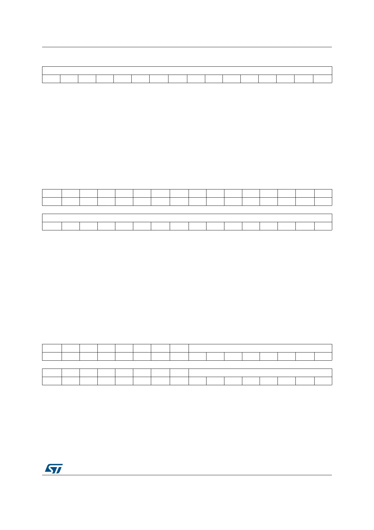
1514131211109 8765432 1 0
PCROP2_STRT[15:0]
rw rw rw rw rw rw rw rw rw rw rw rw rw rw rw rw
Bits 31:16 Reserved, must be kept cleared
Bits 15:0 PCROP2_STRT: Bank 2 PCROP area start offset
PCROP2_STRT contains the first double-word of the Bank 2 PCROP area.
31 30 29 28 27 26 25 24 23 22 21 20 19 18 17 16
Res. Res. Res. Res. Res. Res. Res. Res. Res. Res. Res. Res. Res. Res. Res. Res.
15 14 13 12 11 10 9 8 7 6 5 4 3 2 1 0
PCROP2_END[15:0]
rw rw rw rw rw rw rw rw rw rw rw rw rw rw rw rw
Bits 31:16 Reserved, must be kept cleared
Bits 15:0 PCROP2_END: Bank 2 PCROP area end offset
PCROP2_END contains the last double-word of the bank 2 PCROP area.
31 30 29 28 27 26 25 24 23 22 21 20 19 18 17 16
Res. Res. Res. Res. Res. Res. Res. Res. WRP2A_END[7:0]
rw rw rw rw rw rw rw rw
15 14 13 12 11 10 9 8 7 6 5 4 3 2 1 0
Res. Res. Res. Res. Res. Res. Res. Res. WRP2A_STRT[7:0]
rw rw rw rw rw rw rw rw
Bits 31:24 Reserved, must be kept cleared
Bits 23:16 WRP2A_END: Bank 2 WRP first area “A” end offset
WRP2A_END contains the last page of the bank 2 WRP first area.
Bits 15:8 Reserved, must be kept cleared
Bits 7:0 WRP2A_STRT: Bank 2 WRP first area “A” start offset
WRP2A_STRT contains the first page of the bank 2 WRP first area.

 Loading...


