DocID024597 Rev 3 97/1693
RM0351 Embedded Flash memory (FLASH)
120
Bank 2 WRP Area A address option bytes
Flash memory address: 0x1FFF F818
ST production value: 0x0000 00FF
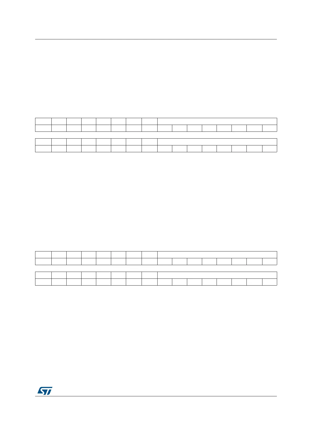
Bank 2 WRP Area B address option bytes
Flash memory address: 0x1FFF F820
ST production value: 0x0000 00FF
3.4.2 Option bytes programming
After reset, the options related bits in the Flash control register (FLASH_CR) are write-
protected. To run any operation on the option bytes page, the option lock bit OPTLOCK in
the Flash control register (FLASH_CR) must be cleared. The following sequence is used to
Bits 31:16 Not used
Bits 15:0 PCROP2_END: Bank 2 PCROP area end offset
PCROP2_END contains the last double-word of the bank 2 PCROP area.
31 30 29 28 27 26 25 24 23 22 21 20 19 18 17 16
Res. Res. Res. Res. Res. Res. Res. Res. WRP2A_END[15:0]
rrrrrrrr
15 14 13 12 11 10 9 8 7 6 5 4 3 2 1 0
Res. Res. Res. Res. Res. Res. Res. Res. WRP2A_STRT[15:0]
rrrrrrrr
Bits 31:24 Not used
Bits 23:16 WRP2A_END: Bank 2 WRP first area “A” end offset
WRP2A_END contains the last page of the Bank 2 WRP first area.
Bits 15:8 Not used
Bits 7:0 WRP2A_STRT: Bank 2 WRP first area “A” start offset
WRP2A_STRT contains the first page of the Bank 2 WRP first area.
31 30 29 28 27 26 25 24 23 22 21 20 19 18 17 16
Res. Res. Res. Res. Res. Res. Res. Res. WRP2B_END[15:0]
rrrrrrrr
15 14 13 12 11 10 9 8 7 6 5 4 3 2 1 0
Res. Res. Res. Res. Res. Res. Res. Res. WRP2B_STRT[15:0]
rrrrrrrr
Bits 31:24 Not used
Bits 23:16 WRP2B_END: Bank 2 WRP first area “B” end offset
WRP2B_END contains the last page of the Bank 2 WRP second area.
Bits 15:8 Not used
Bits 7:0 WRP2B_STRT: Bank 2 WRP first area “B” start offset
WRP2B_STRT contains the first page of the Bank 2 WRP second area.