Embedded Flash memory (FLASH) RM0351
96/1693 DocID024597 Rev 3
Bank 1 WRP Area B address option bytes
Flash memory address: 0x1FFF 7820
ST production value: 0x0000 00FF
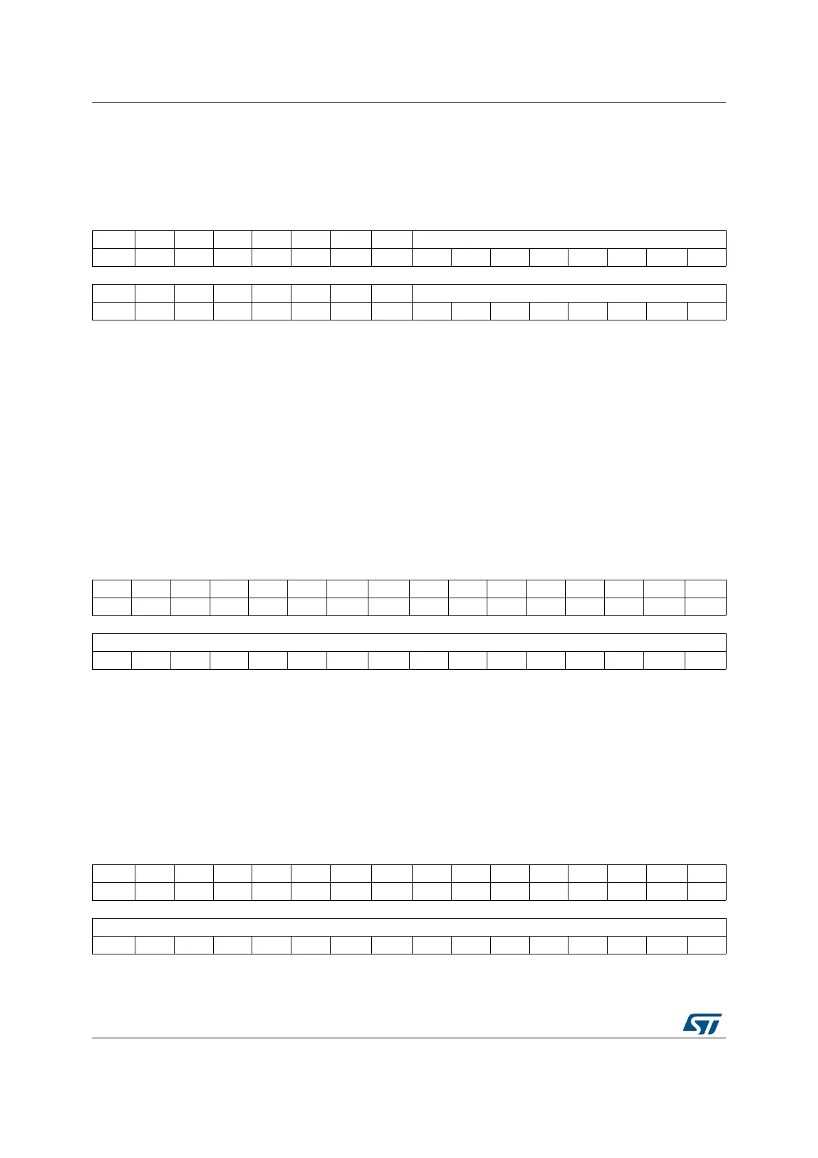
Bank 2 PCROP Start address option bytes
Flash memory address: 0x1FFF F808
ST production value: 0xFFFF FFFF
Bank 2 PCROP End address option bytes
Flash memory address: 0x1FFF F810
ST production value: 0x0000 0000
31 30 29 28 27 26 25 24 23 22 21 20 19 18 17 16
Res. Res. Res. Res. Res. Res. Res. Res. WRP1B_END[15:0]
rrrrrrrr
15 14 13 12 11 10 9 8 7 6 5 4 3 2 1 0
Res. Res. Res. Res. Res. Res. Res. Res. WRP1B_STRT[15:0]
rrrrrrrr
Bits 31:24 Not used
Bits 23:16 WRP1B_END: Bank 1 WRP first area “B” end offset
WRPB1_END contains the last page of the Bank 1 WRP second area.
Bits 15:8 Not used
Bits 7:0 WRP1B_STRT: Bank 1 WRP first area “B” start offset
WRPB1_STRT contains the first page of the Bank 1 WRP second area.
31 30 29 28 27 26 25 24 23 22 21 20 19 18 17 16
Res. Res. Res. Res. Res. Res. Res. Res. Res. Res. Res. Res. Res. Res. Res. Res.
1514131211109 8765432 1 0
PCROP2_STRT[15:0]
rrrrrr r r rrrrrr r r
Bits 31:16 Not used
Bits 15:0 PCROP2_STRT: Bank 2 PCROP area start offset
PCROP2_STRT contains the first double-word of the bank 2 PCROP area.
31 30 29 28 27 26 25 24 23 22 21 20 19 18 17 16
Res. Res. Res. Res. Res. Res. Res. Res. Res. Res. Res. Res. Res. Res. Res. Res.
15 14 13 12 11 10 9 8 7 6 5 4 3 2 1 0
PCROP2_END[15:0]
r rrrrr r r rrrrrr rr
 Loading...


