Power control (PWR) RM0351
174/1693 DocID024597 Rev 3
Access: Additional APB cycles are needed to access this register vs. a standard APB
access (3 for a write and 2 for a read).
5.4.20 Power Port G pull-up control register (PWR_PUCRG)
Address offset: 0x50.
Reset value: 0x0000 0000. This register is not reset when exiting Standby modes and with
PWRRST bit in the RCC_APB1RSTR1 register.
Access: Additional APB cycles are needed to access this register vs. a standard APB
access (3 for a write and 2 for a read).
5.4.21 Power Port G pull-down control register (PWR_PDCRG)
Address offset: 0x54.
Reset value: 0x0000 0000. This register is not reset when exiting Standby modes and with
PWRRST bit in the RCC_APB1RSTR1 register.
Access: Additional APB cycles are needed to access this register vs. a standard APB
access (3 for a write and 2 for a read).
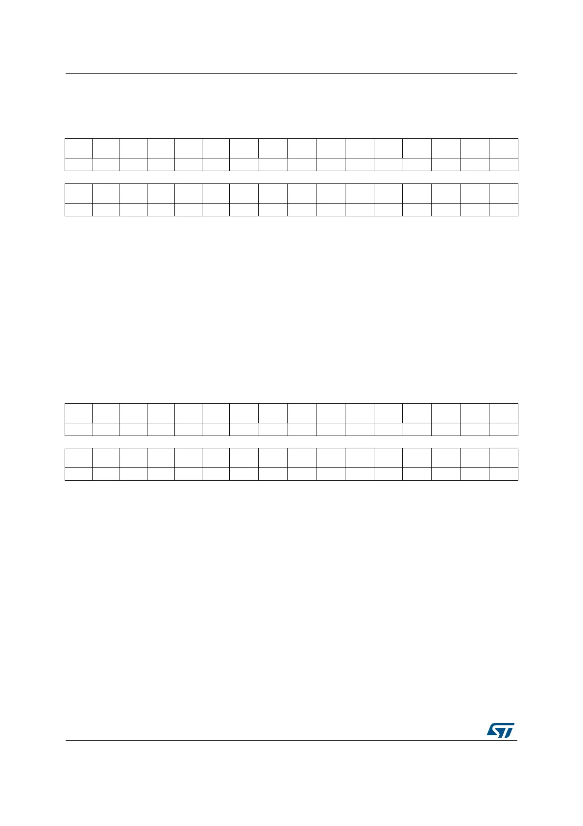
31 30 29 28 27 26 25 24 23 22 21 20 19 18 17 16
Res. Res. Res. Res. Res. Res. Res. Res. Res. Res. Res. Res. Res. Res. Res. Res.
1514131211109876543210
PD15 PD14 PD13 PD12 PD11 PD10 PD9 PD8 PD7 PD6 PD5 PD4 PD3 PD2 PD1 PD0
rw rw rw rw rw rw rw rw rw rw rw rw rw rw rw rw
Bits 31:16 Reserved, must be kept at reset value.
Bits 15:0 PDy: Port F pull-down bit y (y=0..15)
When set, this bit activates the pull-down on PF[y] when APC bit is set in PWR_CR3 register.
31 30 29 28 27 26 25 24 23 22 21 20 19 18 17 16
Res. Res. Res. Res. Res. Res. Res. Res. Res. Res. Res. Res. Res. Res. Res. Res.
1514131211109876543210
PU15 PU14 PU13 PU12 PU11 PU10 PU9 PU8 PU7 PU6 PU5 PU4 PU3 PU2 PU1 PU0
rw rw rw rw rw rw rw rw rw rw rw rw rw rw rw rw
Bits 31:16 Reserved, must be kept at reset value.
Bits 15:0 PUy: Port G pull-up bit y (y=0..15)
When set, this bit activates the pull-up on PG[y] when APC bit is set in PWR_CR3 register.
The pull-up is not activated if the corresponding PDy bit is also set.