Liquid crystal display controller (LCD) RM0351
662/1693 DocID024597 Rev 3
addition, a dedicated blink prescaler selects the blink frequency. This frequency is defined
as:
f
BLINK
= f
ck_div
/2
(BLINKF + 3)
,
with BLINKF[2:0] = 0, 1, 2, ... ,7
The blink frequency achieved is in the range of 0.5 Hz, 1 Hz, 2 Hz or 4 Hz.
22.3.3 Common driver
Common signals are generated by the common driver block (see Figure 153).
COM signal bias
Each COM signal has identical waveforms, but different phases. It has its max amplitude
V
LCD
or V
SS
only in the corresponding phase of a frame cycle, while during the other
phases, the signal amplitude is:
• 1/4 V
LCD
or 3/4 V
LCD
in case of 1/4 bias
• 1/3 V
LCD
or 2/3 V
LCD
in case of 1/3 bias
• and 1/2 V
LCD
in case of 1/2 bias.
Selection between 1/2, 1/3 and 1/4 bias mode can be done through the BIAS bits in the
LCD_CR register.
A pixel is activated when both of its corresponding common and segment lines are active
during the same phase, it means when the voltage difference between common and
segment is maximum during this phase. Common signals are phase inverted in order to
reduce EMI. As shown in Figure 154, with phase inversion, there is a mean voltage of 1/2
V
LCD
at the end of every odd cycle.
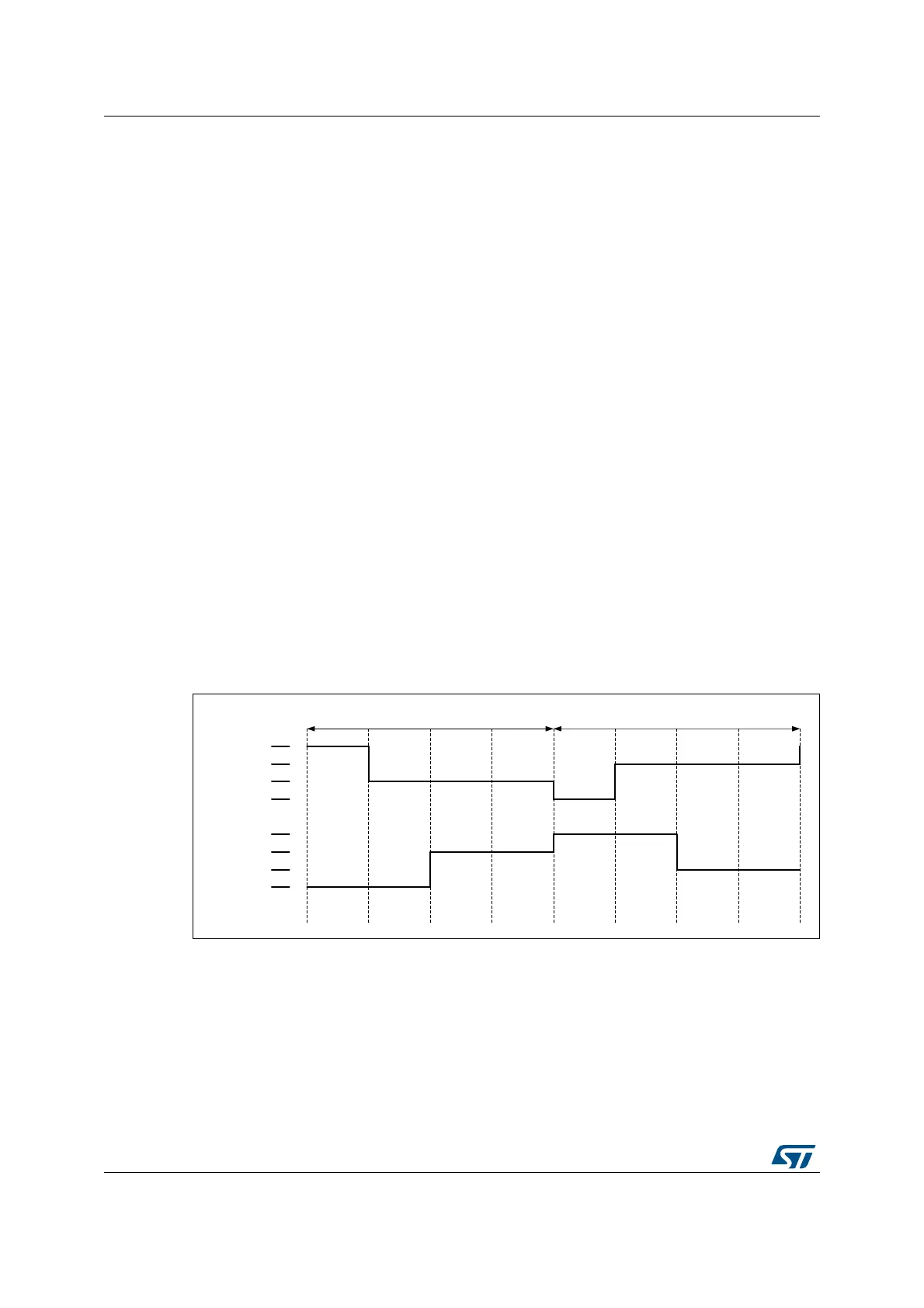
Figure 154. 1/3 bias, 1/4 duty
In case of 1/2 bias (BIAS = 01) the VLCD pin generates an intermediate voltage equal to 1/2
V
LCD
on node b for odd and even frames (see Figure 157).
COM signal duty
Depending on the DUTY[2:0] bits in the LCD_CR register, the COM signals are generated
with static duty (see Figure 156), 1/2 duty (see Figure 157), 1/3 duty (see Figure 158), 1/4
duty (see Figure 159) or 1/8 duty (see Figure 160).
069
9
/&'
2GGIUDPH (YHQIUDPH
&RPDFWLYH
&RPLQDFWLYH &RPLQDFWLYH &RPLQDFWLYH &RPDFWLYH &RPLQDFWLYH &RPLQDFWLYH &RPLQDFWLYH
9
/&'
9
/&'
9
66
9
/&'
9
/&'
9
/&'
9
66
&RPDFWLYH &RPDFWLYH &RPLQDFWLYH &RPLQDFWLYH &RPDFWLYH &RPDFWLYH &RPLQDFWLYH &RPLQDFWLYH
3KDVH 3KDVH 3KDVH 3KDVH 3KDVH 3KDVH 3KDVH 3KDVH
6HJPHQW &RPPRQ

 Loading...


