DocID024597 Rev 3 1311/1685
RM0351 Serial peripheral interface (SPI)
1317
38.6.2 SPI control register 2 (SPIx_CR2)
Address offset: 0x04
Reset value: 0x0700
Bit 2 MSTR: Master selection
0: Slave configuration
1: Master configuration
Note: This bit should not be changed when communication is ongoing.
Bit1 CPOL: Clock polarity
0: CK to 0 when idle
1: CK to 1 when idle
Note: This bit should not be changed when communication is ongoing.
This bit is not used in SPI TI mode.
Bit 0 CPHA: Clock phase
0: The first clock transition is the first data capture edge
1: The second clock transition is the first data capture edge
Note: This bit should not be changed when communication is ongoing.
This bit is not used in SPI TI mode.
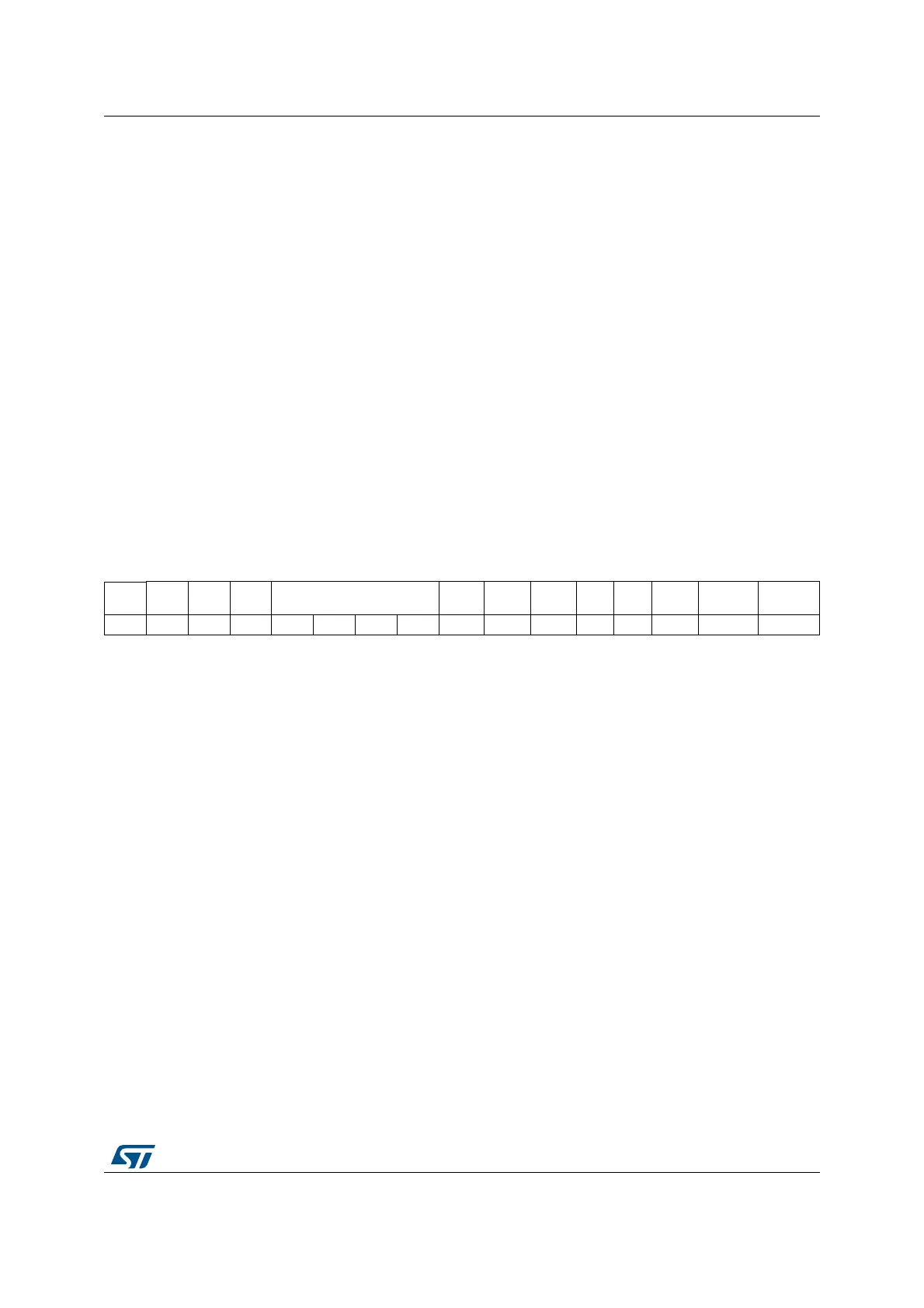
15 14 13 12 11 10 9 8 7 6 5 4 3 2 1 0
Res.
LDMA
_TX
LDMA
_RX
FRXT
H
DS [3:0] TXEIE RXNEIE ERRIE FRF NSSP SSOE TXDMAEN RXDMAEN
rw rw rw rw rw rw rw rw rw rw rw rw rw rw rw
Bit 15 Reserved, must be kept at reset value.
Bit 14 LDMA_TX: Last DMA transfer for transmission
This bit is used in data packing mode, to define if the total number of data to transmit by DMA
is odd or even. It has significance only if the TXDMAEN bit in the SPIx_CR2 register is set and
if packing mode is used (data length =< 8-bit and write access to SPIx_DR is 16-bit wide). It
has to be written when the SPI is disabled (SPE = 0 in the SPIx_CR1 register).
0: Number of data to transfer is even
1: Number of data to transfer is odd
Note: Refer to Procedure for disabling the SPI on page 1294 if the CRCEN bit is set.
Bit 13 LDMA_RX: Last DMA transfer for reception
This bit is used in data packing mode, to define if the total number of data to receive by DMA is
odd or even. It has significance only if the RXDMAEN bit in the SPIx_CR2 register is set and if
packing mode is used (data length =< 8-bit and write access to SPIx_DR is 16-bit wide). It has
to be written when the SPI is disabled (SPE = 0 in the SPIx_CR1 register).
0: Number of data to transfer is even
1: Number of data to transfer is odd
Note: Refer to Procedure for disabling the SPI on page 1294 if the CRCEN bit is set.
Bit 12 FRXTH: FIFO reception threshold
This bit is used to set the threshold of the RXFIFO that triggers an RXNE event
0: RXNE event is generated if the FIFO level is greater than or equal to 1/2 (16-bit)
1: RXNE event is generated if the FIFO level is greater than or equal to 1/4 (8-bit)

 Loading...


