USB on-the-go full-speed (OTG_FS) RM0351
1498/1693 DocID024597 Rev 3
43.4 USB OTG functional description
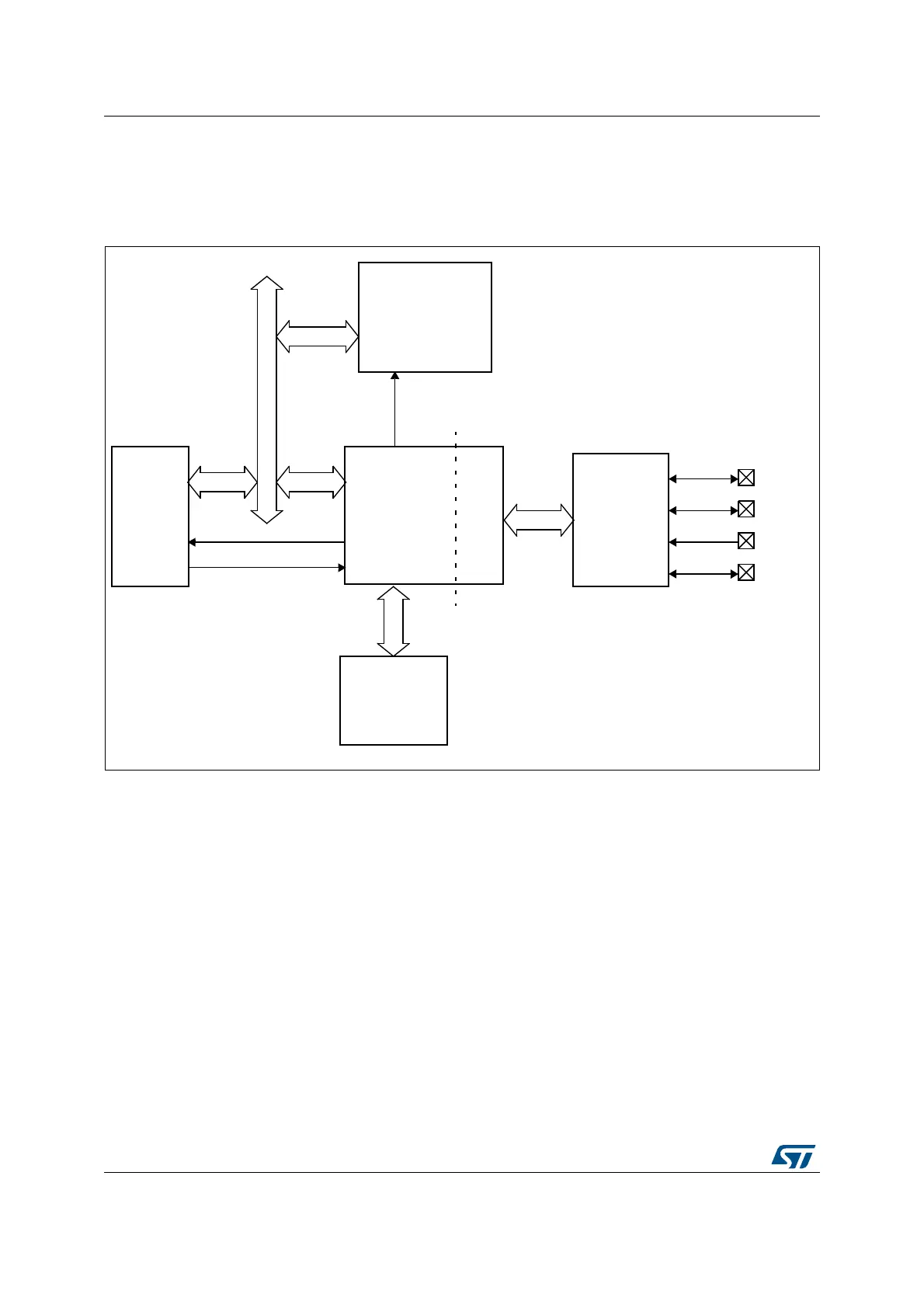
43.4.1 USB OTG block diagram
Figure 493. OTG full-speed block diagram
43.4.2 OTG core
The USB OTG receives the 48 MHz ±0.25% clock from the reset and clock controller
(RCC), via an external quartz. The USB clock is used for driving the 48 MHz domain at full-
speed (12 Mbit/s) and must be enabled prior to configuring the OTG core.
The CPU reads and writes from/to the OTG core registers through the AHB peripheral bus.
It is informed of USB events through the single USB OTG interrupt line described in
Section 43.13: OTG_FS interrupts.
The CPU submits data over the USB by writing 32-bit words to dedicated OTG locations
(push registers). The data are then automatically stored into Tx-data FIFOs configured
within the USB data RAM. There is one Tx FIFO push register for each in-endpoint
(peripheral mode) or out-channel (host mode).
The CPU receives the data from the USB by reading 32-bit words from dedicated OTG
addresses (pop registers). The data are then automatically retrieved from a shared Rx FIFO
configured within the 1.25 KB USB data RAM. There is one Rx FIFO pop register for each
out-endpoint or in-channel.
$0
$-
)$
6
"53
/4'
&3
0(9
53"
/4'&3
#ORE
54-)&3
+BYTES
53"DATA
&)&/S
!("0ERIPHERAL
0OWER
#LOCK
#42,
53")NTERRUPT
53"SUSPEND
53"#LOCKAT-(Z
#ORTEXCORE
3YSTEMCLOCK
DOMAIN
53"CLOCK
DOMAIN
5NIVERSALSERIALBUS
2!-BUS
-36

 Loading...


