Reset and clock control (RCC) RM0351
200/1693 DocID024597 Rev 3
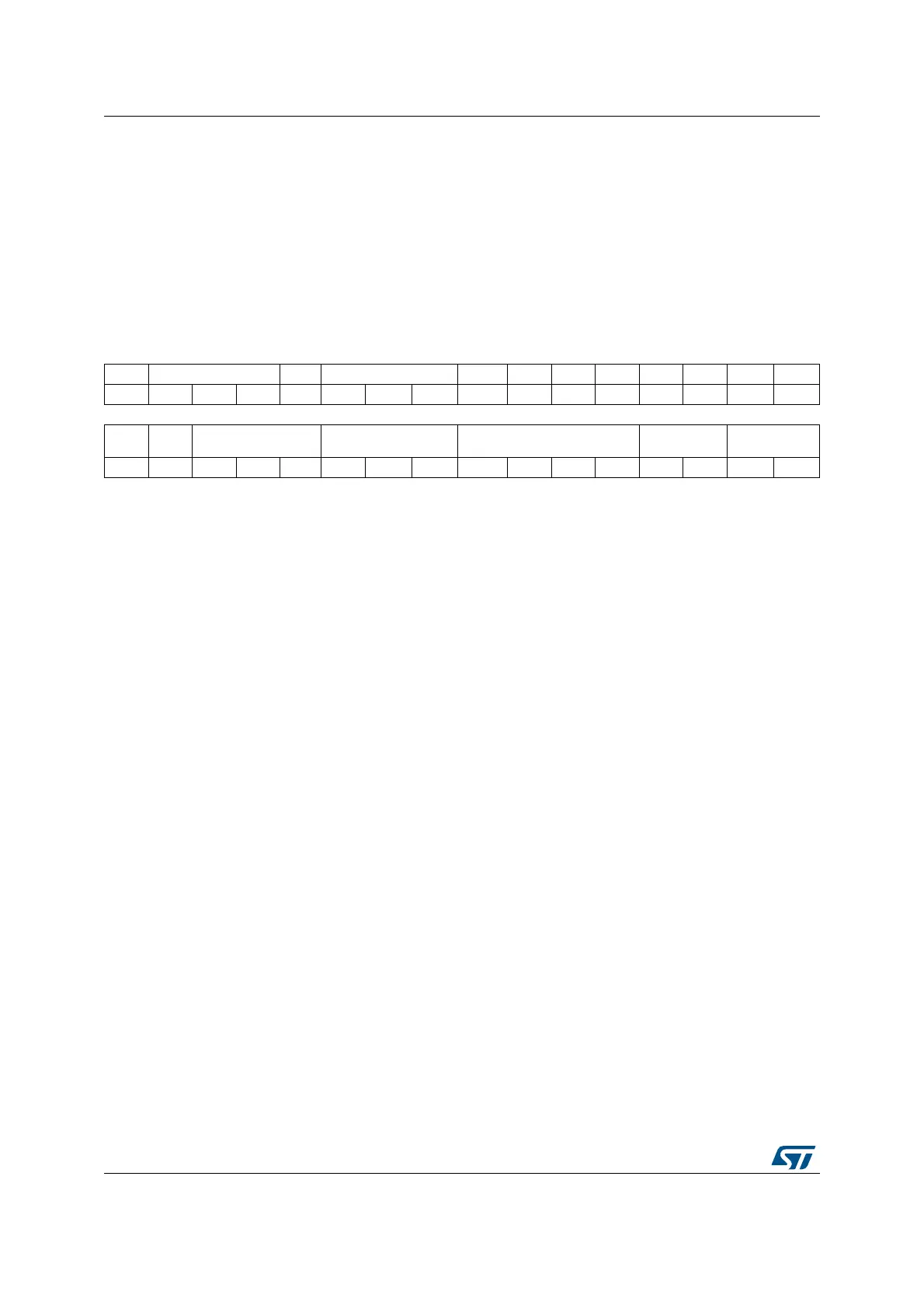
6.4.3 Clock configuration register (RCC_CFGR)
Address offset: 0x08
Reset value: 0x0000 0000
Access: 0 ≤ wait state ≤ 2, word, half-word and byte access
1 or 2 wait states inserted only if the access occurs during clock source switch.
From 0 to 15 wait states inserted if the access occurs when the APB or AHB prescalers
values update is on going.
31 30 29 28 27 26 25 24 23 22 21 20 19 18 17 16
Res. MCOPRE[2:0] Res. MCOSEL[2:0] Res. Res. Res. Res. Res. Res. Res. Res.
rw rw rw rw rw rw
1514131211109 8 7 654321 0
STOP
WUCK
Res. PPRE2[2:0] PPRE1[2:0] HPRE[3:0] SWS[1:0] SW[1:0]
rw rw rw rw rw rw rw rw rw rw rw r r rw rw
Bit 31 Reserved, must be kept at reset value.
Bits 30:28 MCOPRE[2:0]: Microcontroller clock output prescaler
These bits are set and cleared by software.
It is highly recommended to change this prescaler before MCO output is enabled.
000: MCO is divided by 1
001: MCO is divided by 2
010: MCO is divided by 4
011: MCO is divided by 8
100: MCO is divided by 16
Others: not allowed
Bit 27 Reserved, must be kept at reset value.
Bits 26:24 MCOSEL[2:0]: Microcontroller clock output
Set and cleared by software.
000: MCO output disabled, no clock on MCO
001: SYSCLK system clock selected
010: MSI clock selected.
011: HSI16 clock selected.
100: HSE clock selected
101: Main PLL clock selected
110: LSI clock selected
111: LSE clock selected
Note: This clock output may have some truncated cycles at startup or during MCO clock
source switching.
Bits 23:16 Reserved, must be kept at reset value.

 Loading...


